
Active load circuit based on fingerprint sensor acquisition array output stage

A fingerprint sensor and active load technology, applied in the field of semiconductor chips, can solve the problems of fingerprint small signal distortion, insufficient reset of collection points, and far away from common nodes, etc., to reduce distortion, shorten reset time, and increase charge discharge speed Effect

Pending Publication Date: 2019-06-14
宁波爱芯微电子有限公司
View PDF0 Cites 0 Cited by
  • Summary
  • Abstract
  • Description
  • Claims
  • Application Information

AI Technical Summary

Problems solved by technology

If there is not enough reset time, it will lead to insufficient reset of the collection points that are far away from the common node and have large parasitic resistance and parasitic capacitance, resulting in distortion of the small fingerprint signal collected and output

Method used


Image

  • Active load circuit based on fingerprint sensor acquisition array output stage
  • Active load circuit based on fingerprint sensor acquisition array output stage
  • Active load circuit based on fingerprint sensor acquisition array output stage

Examples


Embodiment Construction

[0027] The following describes several preferred embodiments of the present invention with reference to the accompanying drawings, so as to make the technical content clearer and easier to understand. The present invention can be embodied in many different forms of embodiments, and the protection scope of the present invention is not limited to the embodiments mentioned herein.

[0028] In the drawings, components with the same structure are denoted by the same numerals, and components with similar structures or functions are denoted by similar numerals. The size and thickness of each component shown in the drawings are shown arbitrarily, and the present invention does not limit the size and thickness of each component. In order to make the illustration clearer, some places in the drawings schematically exaggerate the thickness of components appropriately.

[0029] In order to improve the collection speed of fingerprint images and reduce the degree of image distortion, the in...


PUM


Abstract

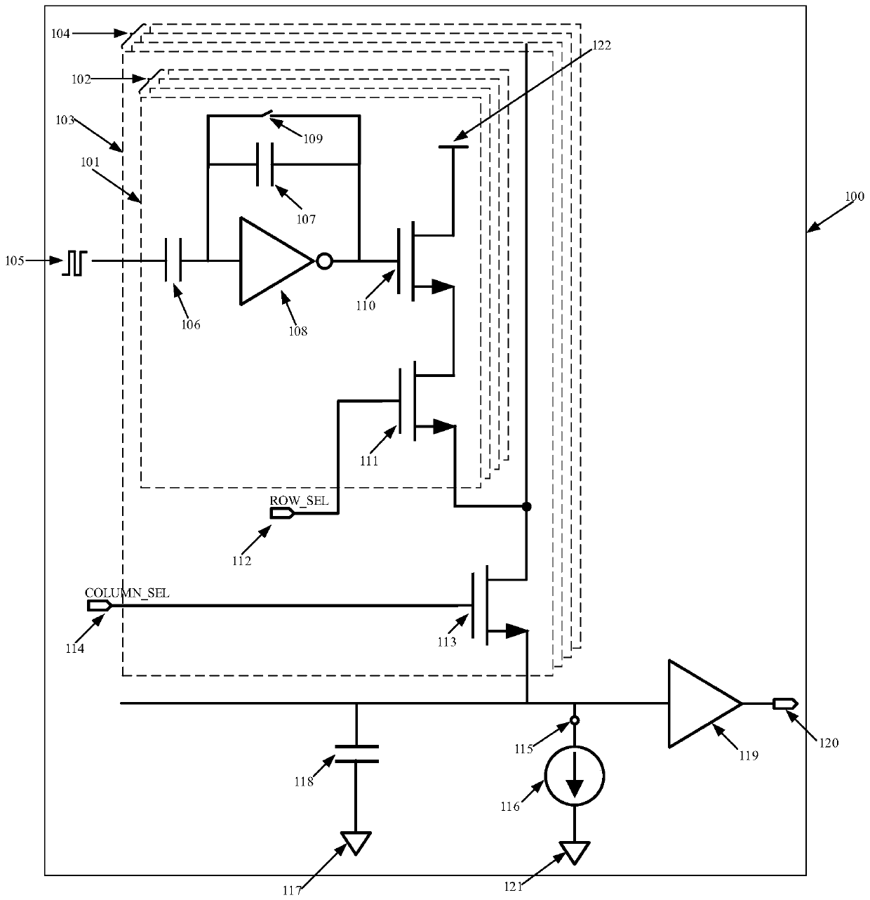
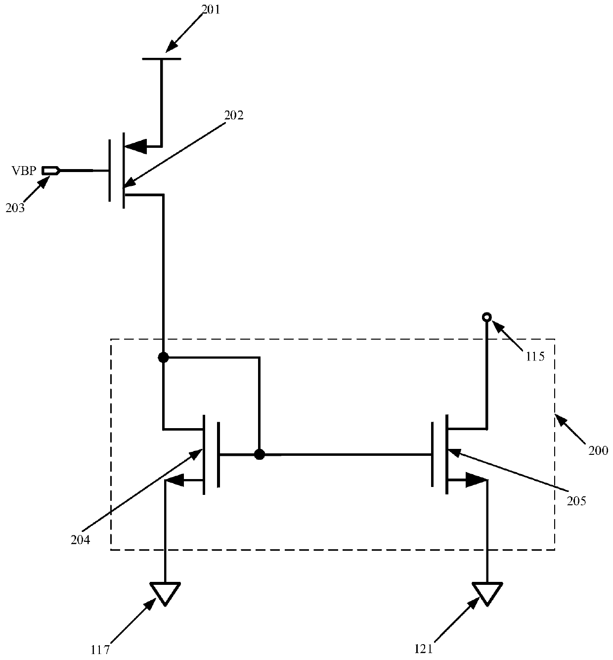
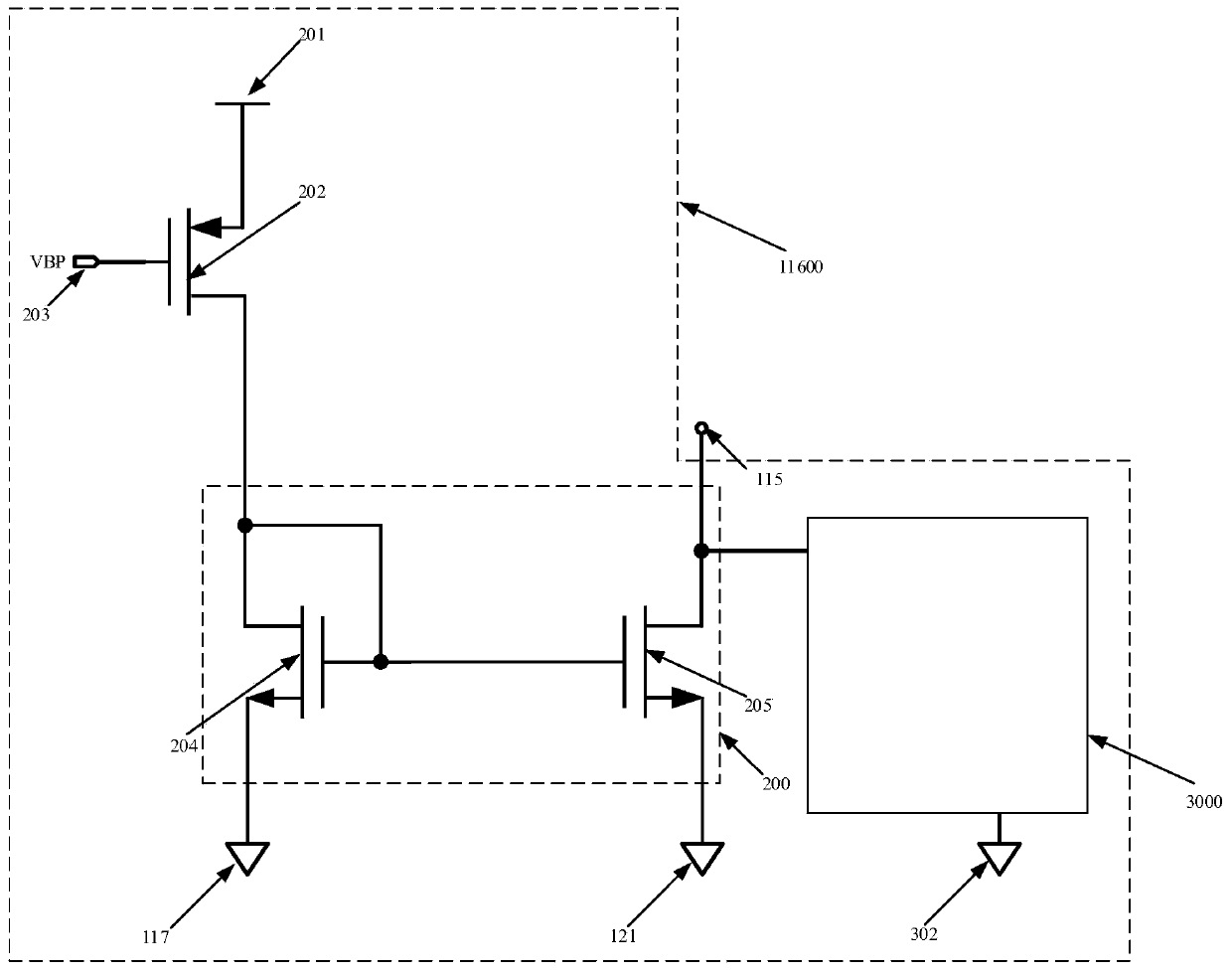
The invention discloses an active load circuit based on a fingerprint sensor acquisition array output stage, and relates to the field of semiconductor chips. The active load circuit comprises a current source and an auxiliary discharge path. The auxiliary discharge path is connected with the current source in parallel. One end of the auxiliary discharge path is connected with a discharge node of the fingerprint sensor collecting array, and the other end is grounded. The active load circuit is improved, and the auxiliary discharge path is added on the basis of the current source, so that the charge discharge speed on the discharge node is increased, the reset time of each acquisition point is shortened, the acquisition speed of fingerprint images is increased, and the distortion degree of the images is reduced.

Description

technical field [0001] The invention relates to the field of semiconductor chips, in particular to an active load circuit of an output stage of a semiconductor fingerprint sensor collection array. Background technique [0002] Most of the existing semiconductor fingerprint sensors are composed of acquisition arrays and signal processing circuits. By point-by-point scanning, the acquisition array converts fingerprint information into analog voltage signals one by one. After filtering, amplification, analog-to-digital conversion and data transmission of the signal processing circuit, the host computer receives the data of each point, according to the acquisition sequence. Perform re-stitching to obtain a grayscale image representing fingerprint information. According to the processing capability, security level and related industry standards of different fingerprint algorithms, the size of the acquisition array is also different. Common acquisition array sizes are 160×160, 19...

Claims


Application Information

Patent Timeline
IPC IPC(8): H03K17/042H03K17/16H03K17/687G06K9/00
Inventor 李富民童红杰
Owner 宁波爱芯微电子有限公司
Learn More