Equivalent circuit of CMOS SPAD photoelectric device
A technology of optoelectronic devices and equivalent circuits, applied in the field of single photon detection
- Summary
- Abstract
- Description
- Claims
- Application Information
AI Technical Summary
Problems solved by technology
Method used
Image

Examples
Embodiment Construction
[0018] The technical solutions in the embodiments of the present invention will be described clearly and in detail below with reference to the drawings in the embodiments of the present invention. The described embodiments are only some of the embodiments of the invention.
[0019] The technical scheme that the present invention solves the problems of the technologies described above is:
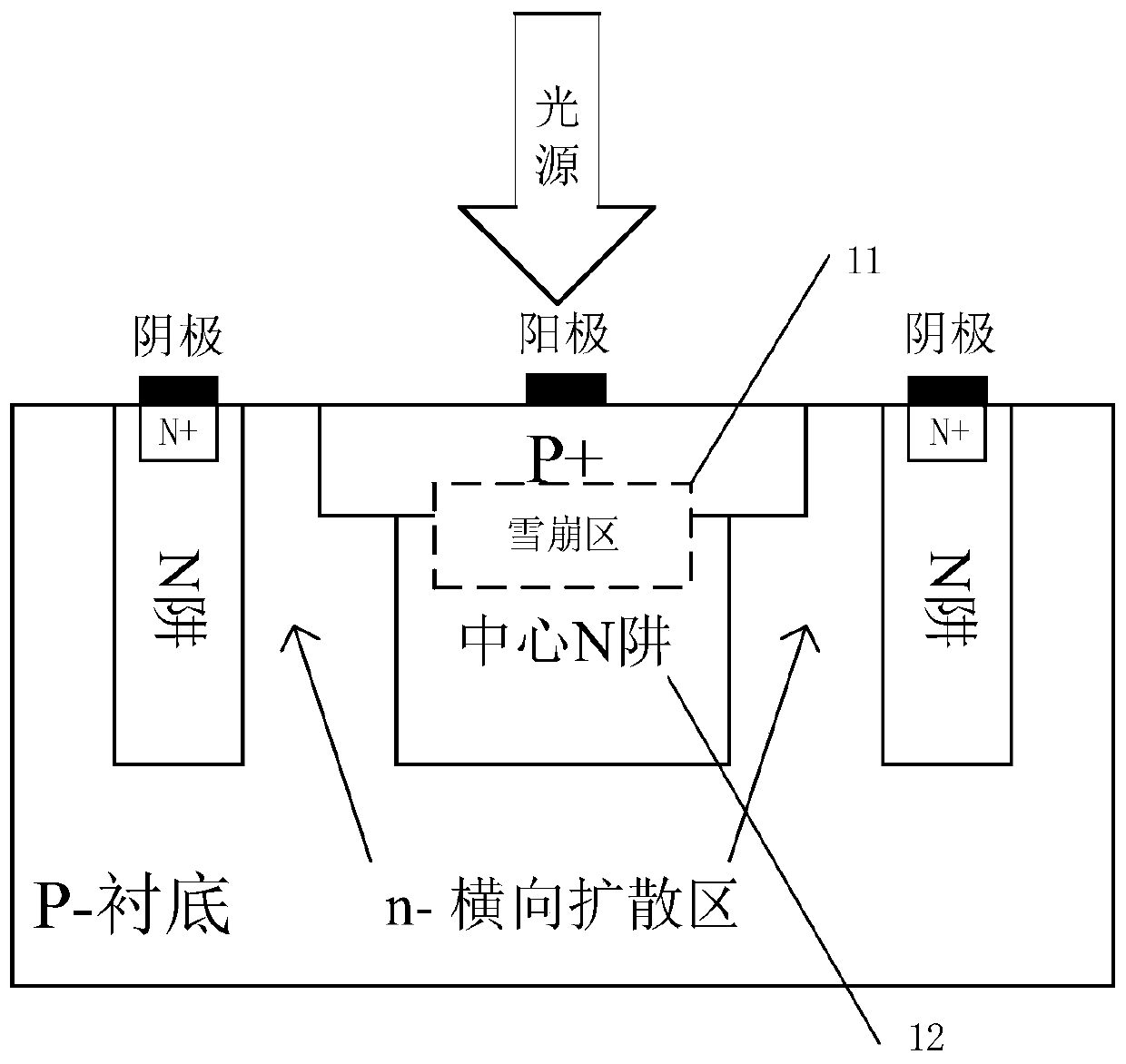
[0020] Such as figure 1 Shown is a block diagram of a CMOS SPAD optoelectronic device. It can be seen from the figure that in this structure, the PN junction is composed of a heavily doped P-type region and a lightly doped N well. The avalanche region (corresponding to region 11 in the figure) is located at the PN junction. The N well below the avalanche region is the main The light absorption area (corresponding to the 12 area in the figure). There is lateral diffusion between the three N wells, resulting in the formation of n at the edge of the PN junction - A virtual guard ring to avo...
PUM
 Abstract
Description
Claims
Application Information
 - R&D
- Intellectual Property
- Life Sciences
- Materials
- Tech Scout
- Unparalleled Data Quality
- Higher Quality Content
- 60% Fewer Hallucinations
Browse by: Latest US Patents, China's latest patents, Technical Efficacy Thesaurus, Application Domain, Technology Topic, Popular Technical Reports.
© 2025 PatSnap. All rights reserved.Legal|Privacy policy|Modern Slavery Act Transparency Statement|Sitemap|About US| Contact US: help@patsnap.com