

Test device and method for detecting bonding strength of semiconductor device
Patent Information
- Authority / Receiving Office
- CN · China
- Patent Type
- Applications(China)
- Current Assignee / Owner
- 深圳市德瑞茵精密科技有限公司
- Publication Date
- 2019-06-25
Smart Images
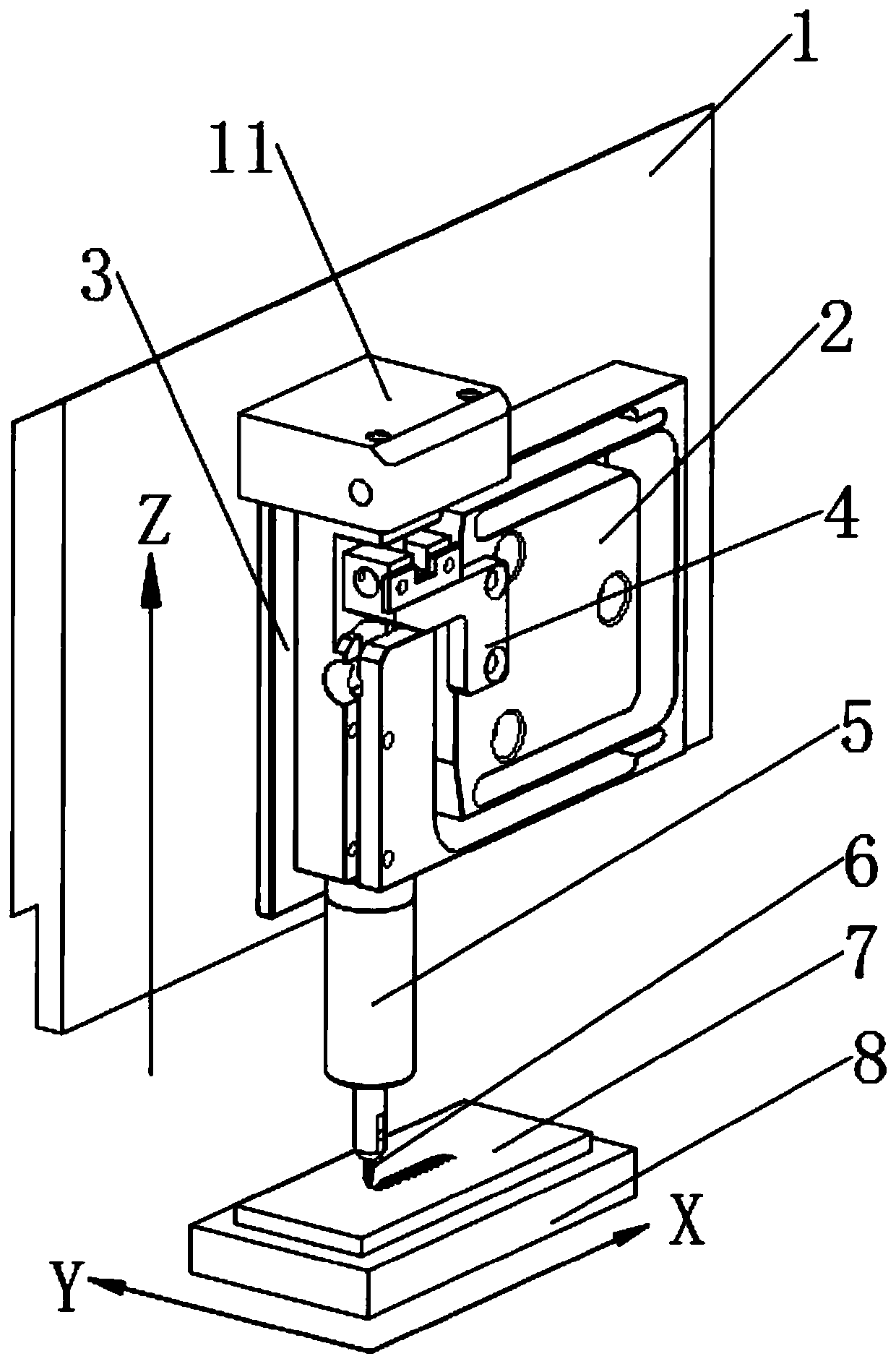
Figure 1 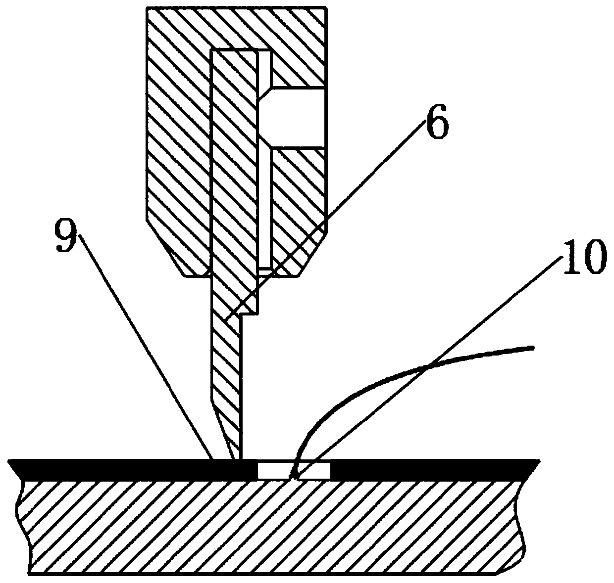
Figure 2 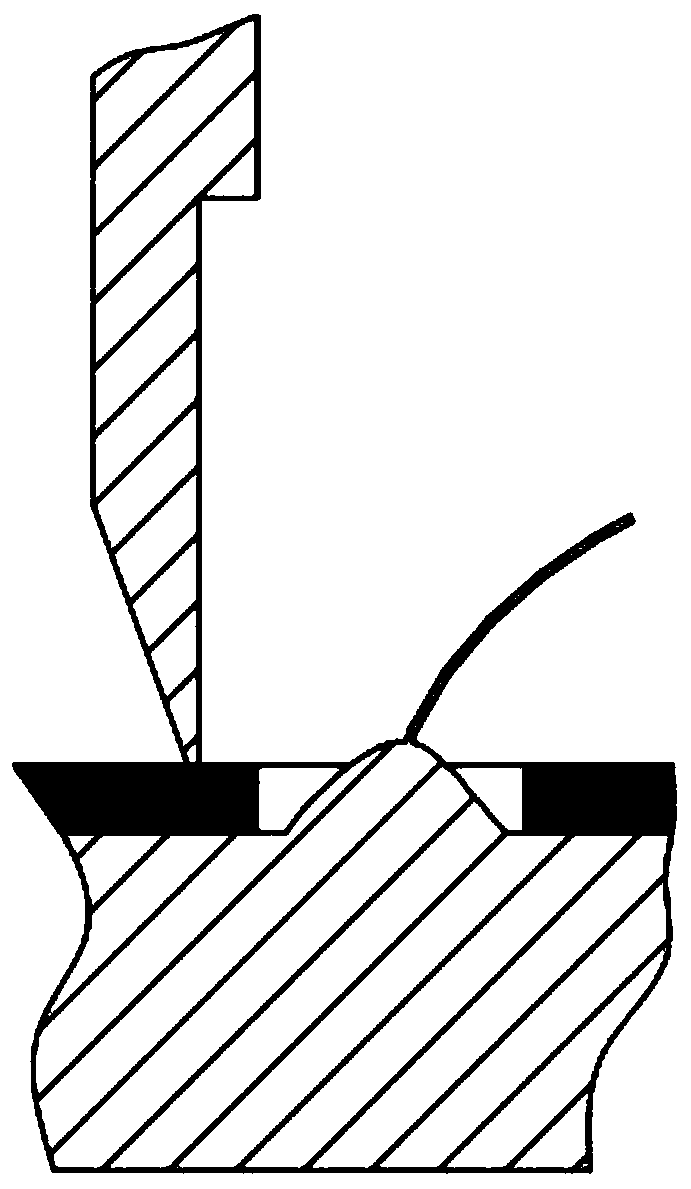
Figure 3
Abstract
Description
Technical field
[0001] The present invention relates to the technical field of semiconductor testing, in particular to a testing device and a testing method for testing the bonding strength of semiconductor devices. Background technique
[0002] With the continuous development of semiconductor technology, more and more functions are integrated on the wafer substrate with a small size, the wiring on the wafer substrate is becoming more and more dense, the circuit stack is more and more, the bonding point of the semiconductor device The circuit layer where the pad is located is under the passivation layer or circuit layer or other protective layer on the surface of the device, and the bonding point pad has a narrow space. Conventional shear testing methods cannot be used, and the test tool must pass through the surface passivation layer or circuit Layers or other protective layers can perform effective bond strength testing.
[0003] Chinese patent application number "ZL201110157669...