Chip transfer substrate and chip transfer method

A chip transfer and substrate technology, which is applied in the manufacture of electrical components, electrical solid devices, semiconductor/solid devices, etc., can solve the problems of chip efficiency, yield rate and transfer accuracy that are difficult to meet the requirements of micro-component production, so as to improve transfer accuracy and Effects of transfer efficiency, improvement of process precision, and reduction of spacing

Active Publication Date: 2019-06-28
BOE TECH GRP CO LTD +1
View PDF13 Cites 10 Cited by
  • Summary
  • Abstract
  • Description
  • Claims
  • Application Information

AI Technical Summary

Problems solved by technology

[0004] In order to solve the above technical problems, the embodiment of the present invention provides a chip transfer substrate and a chip transfer method to solve the problem that the efficiency, yield rate and transfer accuracy of mass transfer of chips are difficult to reach the level of micro components in the production process of existing micro components. production request question

Method used


Image

  • Chip transfer substrate and chip transfer method
  • Chip transfer substrate and chip transfer method
  • Chip transfer substrate and chip transfer method

Examples


Embodiment Construction

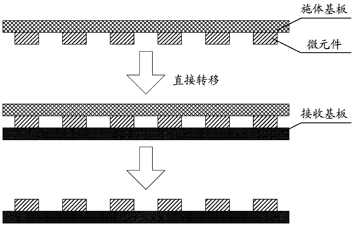
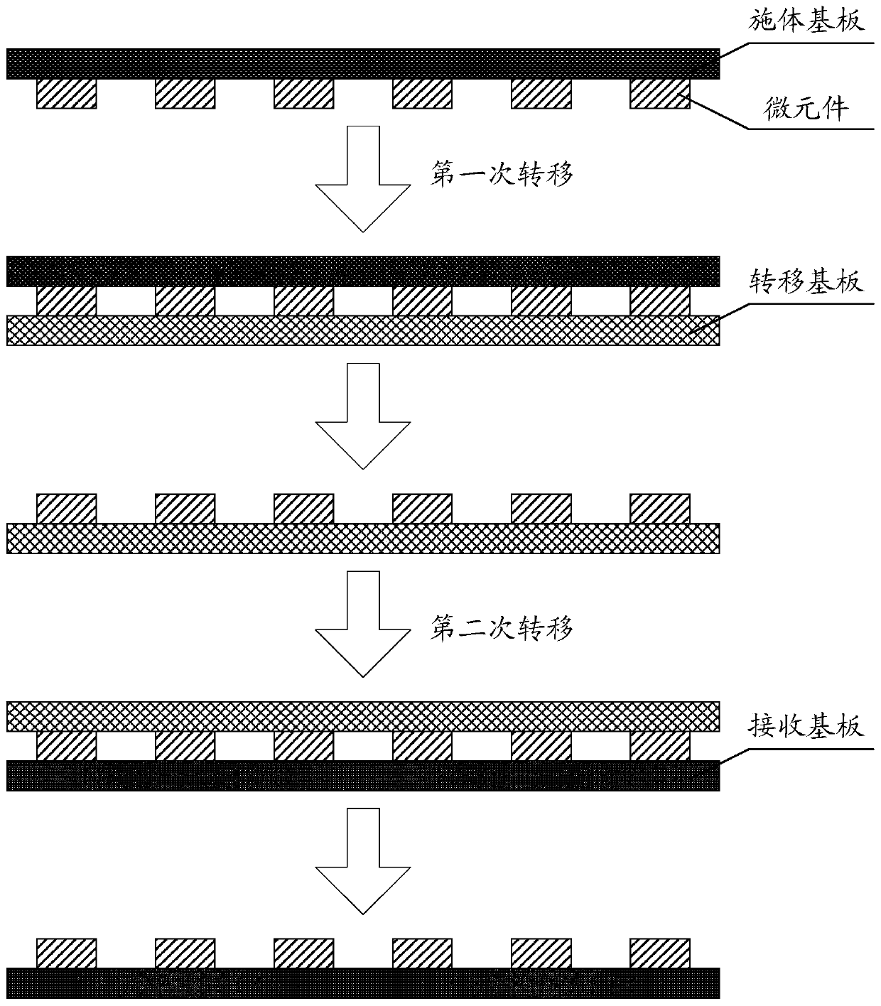
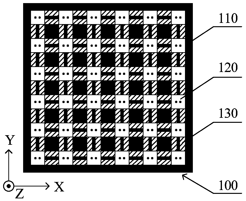
[0052] In order to make the purpose, technical solution and advantages of the present invention more clear, the embodiments of the present invention will be described in detail below in conjunction with the accompanying drawings. It should be noted that, in the case of no conflict, the embodiments in the present application and the features in the embodiments can be combined arbitrarily with each other.

[0053]In addition to the liquid crystal display (Liquid Crystal Display, referred to as: LCD) technology, self-luminous organic electroluminescent display (Organic Light-Emitting Diode, referred to as: OLED) technology, Mirco-LED technology and other technologies are developing rapidly. , Great potential to replace LCD. Micro-LED technology is a display technology that miniaturizes and matrixes the traditional structure, and uses integrated circuit technology to produce a driving circuit to realize the addressing control and individual driving of each pixel. Because the brig...


PUM


Abstract

An embodiment of the present invention discloses a chip transfer substrate and a chip transfer method. The chip transfer substrate comprises a first base layer, chip bases arranged on the first base layer, and a stretching film layer disposed between adjacent chip bases, wherein the stretching film layer is used for generating extension deformation in performing a first operation and generating contraction deformation in performing a second operation. According to the embodiment of the invention, the problem that the efficiency, the yield rate and the transfer precision of the mass transfer ofchips are difficult to meet micro component manufacturing requirements in an existing micro component manufacturing process is solved.

Description

technical field [0001] The present application relates to but not limited to the fields of display technology and semiconductor process technology, especially a chip transfer substrate and a chip transfer method. Background technique [0002] With the development of display technology, the manufacturing process of micro-components has become a development trend of the display panel, such as micro-light emitting diode (Light Emitting Diode, referred to as: LED) (ie, Mirco-LED) technology. [0003] In the fabrication process of microcomponents, the microcomponents should be formed on the donor substrate first, and then transferred to the receiving substrate. Based on the current process manufacturing foundation, there are relatively mature process methods for making thin film transistor (Thin film transistor, abbreviated as: TFT) arrays, Mirco-LED chips and driver integrated circuit (abbreviated as: IC) chips; however , The mass transfer of Mirco-LED chips is a difficult poin...

Claims


Application Information

Patent Timeline
Patent Type & Authority Applications(China)
IPC IPC(8): H01L21/683H01L25/075H01L33/00
Inventor 杨啸剑郑辉张明辉朴仁镐崔晓鹏
Owner BOE TECH GRP CO LTD
Why Eureka
Try Eureka