A kind of based on cesium lead iodine photodetector and preparation method

A photodetector, cesium lead technology, applied in the field of photodetectors, can solve the problems of device performance failure, easy decomposition and phase change, etc., and achieve the effect of good device performance, simple preparation process and high stability

Active Publication Date: 2021-02-02
湖北安一辰光电科技有限公司
View PDF4 Cites 1 Cited by
  • Summary
  • Abstract
  • Description
  • Claims
  • Application Information

AI Technical Summary

Problems solved by technology

Cesium lead iodine quantum dots synthesized by liquid phase method are easy to decompose and phase change in the process of device preparation, resulting in failure of device performance

Method used


Image

  • A kind of based on cesium lead iodine photodetector and preparation method

Examples


Embodiment 1

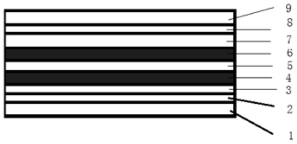
[0017] Embodiment one: on the substrate layer of silicon with oxide layer grown on the surface, adopt the chemical vapor deposition method to deposit lead iodide PbI with a thickness of 2 nanometers on the electrode layer surface successively 2 layer, further deposited on it with a thickness of 2 nanometers of cesium iodide CsI layer, and then deposited and grown with a thickness of 2 nanometers of lead iodide layer; Two layers of perovskite cesium lead iodide CsPbI with a thickness of 2 nm were obtained at the two interface layers 3 A photosensitive layer; then an electrode with a thickness of 20 nanometers is evaporated on the surface of the lead iodide; finally, a protective layer of polymethyl methacrylate PMMA device is spin-coated on the surface of the electrode layer, and the thickness of the protective layer is 20 nanometers.

Embodiment 2

[0018] Embodiment two: on the glass sheet substrate layer, adopt the chemical vapor deposition method, deposit the lead iodide PbI that thickness is 2 nanometers successively on the electrode layer surface 2 layer, further deposited on it with a thickness of 2 nanometers of cesium iodide CsI layer, and then deposited and grown with a thickness of 2 nanometers of lead iodide layer; Two layers of perovskite cesium lead iodide CsPbI with a thickness of 8 nm were obtained at the two interface layers 3 photosensitive layer; then evaporate an electrode with a thickness of 50 nanometers on the surface of lead iodide; finally spin-coat a polymethyl methacrylate PMMA device protection layer on the surface of the electrode layer, and the thickness of the protection layer is 50 nanometers.

Embodiment 3

[0019] Embodiment three: above the substrate layer of the silicon that surface grows oxide layer, adopt chemical vapor deposition method, deposit the lead iodide PbI that thickness is 5 nanometers successively on electrode layer surface 2 layer, further deposited on it with a thickness of 2 nanometers of cesium iodide CsI layer, and then deposited and grown with a thickness of 2 nanometers of lead iodide layer; Two layers of perovskite cesium lead iodide CsPbI with a thickness of 3 nm were obtained at the two interface layers 3 A photosensitive layer; then an electrode with a thickness of 40 nanometers is evaporated on the surface of the lead iodide; finally, a protective layer of polymethyl methacrylate PMMA device is spin-coated on the surface of the electrode layer, and the thickness of the protective layer is 40 nanometers.


PUM


Abstract

The invention discloses a cesium lead iodine photoelectric detector and a preparation method thereof. The photoelectric detector successively comprises, from bottom to top, a substrate layer, a firstelectrode layer, a perovskite cesium lead iodine photosensitive layer, a second electrode layer and a device protective layer. The perovskite cesium lead iodine photosensitive layer has a thickness of10 to 22nm, and successively comprises, from bottom to top, a first lead iodide layer, a first perovskite cesium lead iodine CsPbI3 photosensitive layer, cesium iodide, a second perovskite cesium lead iodine CsPbI3 photosensitive layer, and a second lead iodine layer. The perovskite cesium lead iodine photosensitive layer is prepared by chemical vapor deposition. In the invention, the cesium iodide and the lead iodide are alternately deposited by chemical vapor deposition so as to chemically react at an interface to form a perovskite cesium lead iodine film layer to form a sandwich structure.Such structure contributes to improvement in the stability of a perovskite cesium lead iodine film.

Description

technical field [0001] The invention belongs to the field of device preparation. Specifically relates to a photodetector based on a perovskite structure cesium lead iodine thin film as a photosensitive layer. Background technique [0002] Cesium lead iodide (CsPbI) perovskite structure 3 ) Quantum dots have high photoelectric conversion efficiency and are used to prepare photodetectors. Cesium lead iodine quantum dots synthesized by liquid phase method are easy to decompose and phase change in the process of device preparation, resulting in failure of device performance. Contents of the invention [0003] Aiming at the deficiencies of the prior art, the invention proposes a preparation method of a cesium-lead-iodine photodetector prototype device. [0004] The perovskite cesium lead iodine photodetector prepared by the invention has simple preparation process, good device performance and high stability. [0005] A cesium-lead-iodine photodetector based on a substrate l...

Claims


Application Information

Patent Timeline
Patent Type & Authority Patents(China)
IPC IPC(8): H01L31/101H01L31/18H01L31/0216H01L31/032
CPCY02P70/50
Inventor 吕燕飞徐竹华赵士超
Owner 湖北安一辰光电科技有限公司
Why Eureka
Try Eureka