Six-side coarsened infrared LED chip and manufacturing method thereof

A technology of LED chip and manufacturing method, which is applied in the direction of electrical components, circuits, semiconductor devices, etc., can solve the problems of excessive energy, loss, and infrared LED chip LED light extraction is not maximized, etc., to improve the bonding strength and increase the life of the chip , The effect of improving light extraction efficiency

Pending Publication Date: 2019-07-02
YANGZHOU CHANGELIGHT
View PDF8 Cites 1 Cited by
  • Summary
  • Abstract
  • Description
  • Claims
  • Application Information

AI Technical Summary

Problems solved by technology

[0003] However, the current infrared LED chip on the GaAs substrate does no

Method used


Image

  • Six-side coarsened infrared LED chip and manufacturing method thereof
  • Six-side coarsened infrared LED chip and manufacturing method thereof
  • Six-side coarsened infrared LED chip and manufacturing method thereof

Examples


Embodiment Construction

[0062] The technical solutions in the embodiments of the present invention will be clearly and completely described below in conjunction with the accompanying drawings in the embodiments of the present invention. Obviously, the described embodiments are only a part of the embodiments of the present invention, rather than all the embodiments. Based on the embodiments of the present invention, all other embodiments obtained by those of ordinary skill in the art without creative work shall fall within the protection scope of the present invention.

[0063] In order to make the above-mentioned objects, features and advantages of the present invention more obvious and easy to understand, the present invention will be further described in detail below in conjunction with the accompanying drawings and specific embodiments.

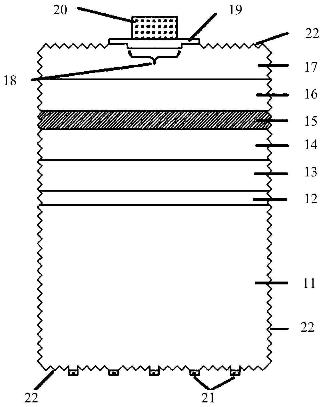
[0064] reference figure 1 , figure 1 It is a schematic structural diagram of a six-sided roughened infrared LED chip provided by an embodiment of the present invention...


PUM

PropertyMeasurementUnit
Thicknessaaaaaaaaaa
Thicknessaaaaaaaaaa
Heightaaaaaaaaaa

Abstract

The invention provides a six-side coarsened infrared LED chip and a manufacturing method thereof. An ITO finger-shaped electrode, instead of the metal finger-shaped electrode, is adopted for current expansion, thereby effectively solving the problem of shading absorption of the metal finger-shaped electrode, and achieving the good current expansion. Moreover, compared with a front ITO current expansion layer, the ITO finger-shaped electrode has the advantages that the surface roughening treatment can be carried out on the area outside the ITO finger-shaped electrode, so that the light extraction efficiency is improved. A Schottky barrier region is arranged below the ITO finger-shaped electrode, so that the current can be preferentially expanded to the periphery of the chip along the ITO finger-shaped electrode, thereby reducing the current directly injected to the lower part of the electrode, and improving the effective injection of the current. Through the grid type N electrode structure, the LED chip can avoid the problem of non-uniform current distribution of the dot-matrix type back electrode, and also can avoid the problem of light absorption of the whole back electrode.

Description

Technical field [0001] The invention relates to the technical field of semiconductor light-emitting diodes, and more specifically, to a six-sided roughened infrared LED chip and a manufacturing method. Background technique [0002] GaAs is a direct bandgap semiconductor with a band gap of 1.42eV. As a substrate material, it is widely used in the growth of AlGaAs-based infrared LED epitaxial wafers. According to its forbidden band width, infrared light with a wavelength greater than 870nm can penetrate the GaAs substrate. [0003] However, the current infrared LED chip LED light extraction on the GaAs substrate is not maximized, and there is still a lot of energy loss. Summary of the invention [0004] In view of this, in order to solve the above problems, the present invention provides a six-sided roughened infrared LED chip and a manufacturing method. The technical solution is as follows: [0005] A six-sided roughened infrared LED chip, the infrared LED chip comprising: [0006] Su...

Claims


Application Information

Patent Timeline
IPC IPC(8): H01L33/00H01L33/20H01L33/38
CPCH01L33/20H01L33/005H01L33/385
Inventor 徐洲王洪占彭钰仁张国庆陈凯轩蔡端俊
Owner YANGZHOU CHANGELIGHT
Why Eureka
Try Eureka