Crystal diameter control method for Czochralski silicon single crystal growth process

A technology of growth process and control method, which is applied in the field of crystal diameter control in the growth process of Czochralski silicon single crystal, can solve the problems of low yield, fluctuation of pulling speed, decline of crystal quality, etc., to achieve reasonable and accurate judgment and shorten the response. Time lag, not easy to effect the large fluctuation of crystal diameter

Active Publication Date: 2019-07-05
ZHEJIANG JINGSHENG MECHANICAL & ELECTRICAL
View PDF2 Cites 7 Cited by
  • Summary
  • Abstract
  • Description
  • Claims
  • Application Information

AI Technical Summary

Problems solved by technology

In the process of controlling the crystal diameter by changing the pulling speed in the traditional process, there is a problem of large fluctuations in t

Method used


Image

  • Crystal diameter control method for Czochralski silicon single crystal growth process
  • Crystal diameter control method for Czochralski silicon single crystal growth process
  • Crystal diameter control method for Czochralski silicon single crystal growth process

Examples


Embodiment 1

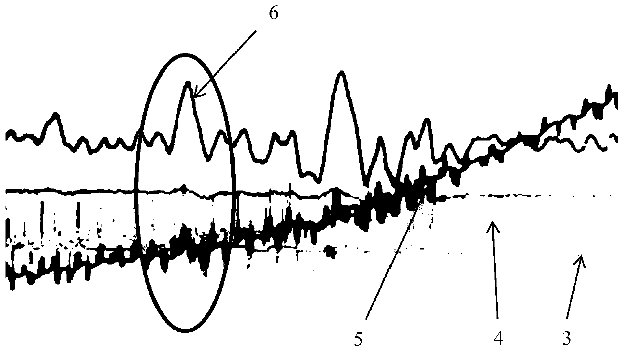
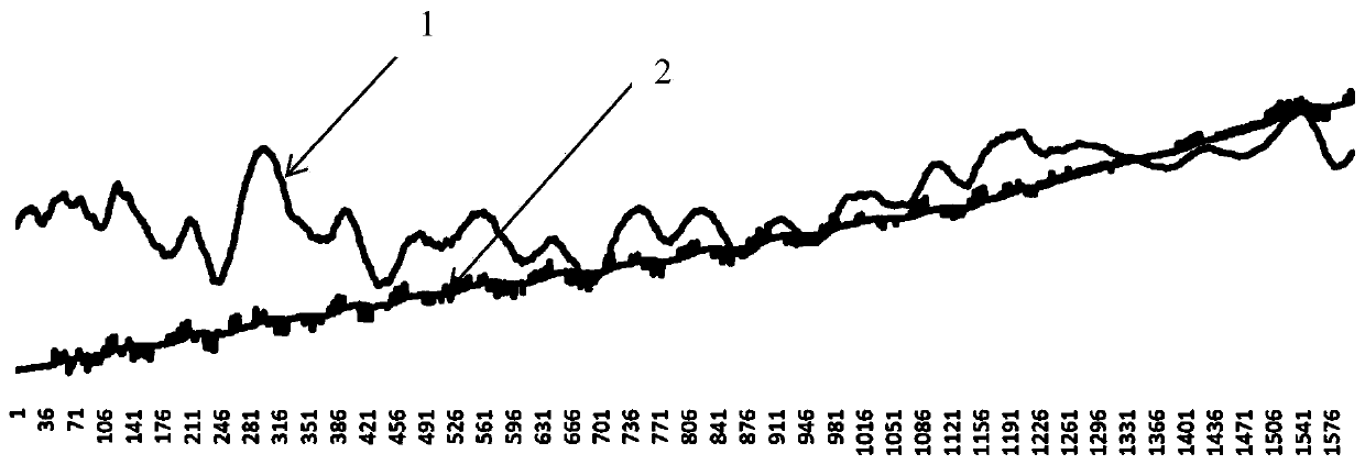
[0047] Use a 24-inch thermal field to grow crystals with a diameter of 210mm, and the loading capacity is 120kg. After the steps of seeding, shouldering and shoulder turning, the crystal enters the equal-diameter growth stage. In the initial stage of crystal isometric growth, there is a large deviation between the set diameter and the target diameter, and the set growth rate and the actual growth rate. When the equal-diameter length of the crystal reaches 100mm, the actual diameter of the crystal is 210.8mm, and the deviation is less than 1mm; the crystal average The growth rate is 33.4-33.8mm / hr, the target growth rate is 35mm / hr, the deviation is less than 2mm / hr, and it is maintained for 15 minutes, and the set point of the thermal field temperature is constant for 20 minutes. It is determined that the diameter control method of the present invention can be implemented.

[0048] To implement the diameter control method of the present invention, the crystal pulling speed is ...

Embodiment 2

[0077] Embodiment 2: Example of control of thermal field temperature

[0078] Use a 24-inch thermal field to grow crystals with a diameter of 210mm, and the loading capacity is 120kg. After the steps of seeding, shouldering and shoulder turning, the crystal enters the equal-diameter growth stage. In the initial stage of crystal isometric growth, there is a large deviation between the set diameter and the target diameter, and the set growth rate and the actual growth rate. When the equal-diameter length of the crystal reaches 100mm, the actual diameter of the crystal is 210.8mm, and the deviation is less than 1mm; the crystal average The growth rate is 33.4-33.8mm / hr, the target growth rate is 35mm / hr, the deviation is less than 2mm / hr, and it is maintained for 15 minutes, and the set point of the thermal field temperature is constant for 20 minutes. It is determined that the diameter control method of the present invention can be implemented.

[0079] To implement the diamete...


PUM


Abstract

The invention relates to a semiconductor crystal manufacturing technology and aims to provide a crystal diameter control method for a Czochralski silicon single crystal growth process. The method comprises the following steps: when a silicon single crystal is produced by a Czochralski method, enabling the crystal to reach a stable state in the equal-diameter growth process; setting the actual pulling speed of the crystal as the current average pulling speed, and making the actual pulling speed close to the set pulling speed according to a preset change rate until the pulling speed of the crystal is constant and does not fluctuate with the diameter of the crystal; in the equal-diameter growth process of the crystal, controlling the diameter of the crystal by adjusting the power of a heater,and particularly adding variable period pulse type power output on the basis of the current heating average power. According to the method, through calculation of crystal diameter change speed and acceleration and critical value control, the key point judgment of power output time is more reasonable and accurate; the response time lag of the diameter change to power regulation can be shortened; the crystal diameter cannot be greatly disturbed, and the crystal diameter cannot easily fluctuate greatly.

Description

technical field [0001] The patent of the invention is applicable to semiconductor crystal manufacturing technology, and specifically relates to a crystal diameter control method used in the Czochralski silicon single crystal growth process. [0002] technical background [0003] In the traditional Czochralski silicon single crystal growth process, the crystal diameter is generally controlled by adjusting the crystal pulling speed. Because the crystal diameter change responds quickly to the adjustment of the pulling speed, a better diameter control effect can be obtained. In order to control and reduce micro-defects in high-end semiconductor-grade silicon single crystals, the consensus in the industry is to achieve this through V / G regulation at the crystal growth interface. Among them, G refers to the temperature gradient at the crystal growth interface, which is mainly determined by the relative position of the growth interface in the thermal field. Because the position of...

Claims


Application Information

Patent Timeline
IPC IPC(8): C30B15/22C30B29/06
CPCC30B15/203C30B15/22C30B29/06
Inventor 高宇胡建荣傅林坚曹建伟夏泽杰王小飞倪军夫叶钢飞谭庆
Owner ZHEJIANG JINGSHENG MECHANICAL & ELECTRICAL
Why Eureka
Try Eureka