
LED chip structure with electrode having opening

An LED chip and electrode technology, applied in circuits, electrical components, semiconductor devices, etc., can solve the problems of light-emitting diode offset, tilt, and large surface tension of light-emitting diodes, and achieve consistent light-emitting directions, improved flatness, and uniform color mixing. Effect

Pending Publication Date: 2019-07-05
XIAMEN QIANZHAO SEMICON TECH CO LTD
View PDF0 Cites 4 Cited by
  • Summary
  • Abstract
  • Description
  • Claims
  • Application Information

AI Technical Summary

Problems solved by technology

[0003] However, when the size of the light-emitting diode is small (such as Mini LED and Micro LED), the solder is melted into a liquid state by high temperature during soldering, and the surface tension of the light-emitting diode is particularly high, and the excess solder is likely to become a protruding sphere, resulting in Light-emitting diodes are prone to problems such as offset and tilt

Method used


Image

  • LED chip structure with electrode having opening
  • LED chip structure with electrode having opening
  • LED chip structure with electrode having opening

Examples


Embodiment 1

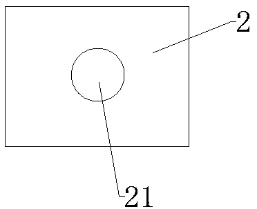
[0039] Such as Figure 10 Shown, embodiment one of the present invention is:

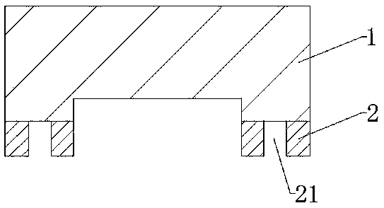
[0040] An LED chip structure with electrodes having openings includes an epitaxial structure 1 and an electrode 2 disposed on the epitaxial structure 1 , the electrode 2 includes a bottom and a top opposite to each other, and a side wall connecting the bottom and the top. The top of the electrode 2 is disposed close to the epitaxial structure 1 , and the bottom of the electrode 2 is disposed away from the epitaxial structure 1 .

[0041] The electrode 2 is provided with more than two openings 21 extending from the bottom of the electrode to the top of the electrode, the opening 21 is in the shape of a circular hole, and the distance between the opening 21 and the side wall of the electrode 2 It is provided that more than two openings 21 are evenly distributed at intervals.

[0042] In a preferred embodiment, the apertures of the openings are gradually reduced from the bottom of the electrode to th...

Embodiment 2

[0043] Such as Figure 11 Shown, embodiment two of the present invention is:

[0044]An LED chip structure with electrodes having openings includes an epitaxial structure 1 and an electrode 2 disposed on the epitaxial structure 1 , the electrode 2 includes a bottom and a top opposite to each other, and a side wall connecting the bottom and the top. The top of the electrode 2 is disposed close to the epitaxial structure 1 , and the bottom of the electrode 2 is disposed away from the epitaxial structure 1 .

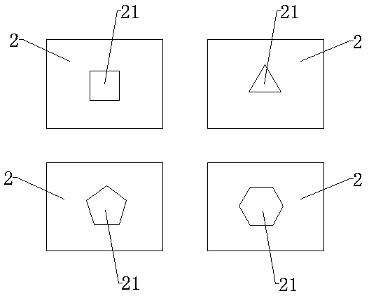
[0045] The electrode 2 is provided with more than two openings 21 extending from the bottom of the electrode 2 to the top of the electrode 2, and more than two openings 21 are evenly distributed at intervals, and the openings 21 are in the shape of trapezoidal grooves The opening 21 communicates with two opposite side walls of the electrode 2 , wherein the cross-sectional area of ​​the opening 21 near the top of the electrode 2 is smaller than the cross-sectional area of ​...

Embodiment 3

[0047] An LED chip structure with an electrode opening includes an epitaxial structure and an electrode arranged on the epitaxial structure, the electrode includes a bottom and a top oppositely arranged, and a side wall connecting the bottom and the top. The top of the electrode is disposed close to the epitaxial structure, and the bottom of the electrode is disposed away from the epitaxial structure.

[0048] The electrode is provided with more than two openings extending from the bottom of the electrode to the top of the electrode, the openings have rough side walls, and the bottom of the openings has a distance from the epitaxial structure.

[0049] This embodiment can also be applied to the first and second embodiments above.

[0050] In an alternative embodiment, the opening extends from the bottom of the electrode to the top of the electrode, communicating with the epitaxial structure.


PUM


Abstract

The invention provides an LED chip structure with an electrode having an opening. The LED chip structure comprises an epitaxial structure and an electrode disposed on the epitaxial structure, the topof the electrode is disposed adjacent to the epitaxial structure, the bottom of the electrode is disposed away from the epitaxial structure, and the electrode is provided with at least one opening extending from the bottom of the electrode toward the top of the electrode. By adsorbing excess solder at the opening of the electrode, a spheroid is prevented from occurring in a soldering process, so that a semiconductor chip generates no phenomenon of offset or tilt caused by the soldering, and the flatness of a light emitting surface is effectively improved. Especially on displays and visualization products, the LED chip structure has the advantages of uniform light emitting direction, uniform color mixing, etc.

Description

technical field [0001] The invention relates to the technical field of light-emitting semiconductors, in particular to an LED chip structure with electrodes having openings. Background technique [0002] Light-emitting diodes are widely used in fields such as living lighting, signal lights, and outdoor full-color large-scale display screens due to their long life, good luminous performance, energy saving and environmental protection. Existing light-emitting diode chips are generally composed of epitaxial structures and electrodes, and the electrodes are welded to external circuits through soldering agents such as solder paste. [0003] However, when the size of the light-emitting diode is small (such as Mini LED and Micro LED), the solder is melted into a liquid state by high temperature during soldering, and the surface tension of the light-emitting diode is particularly high, and the excess solder is likely to become a protruding sphere, resulting in Light-emitting diodes...

Claims


Application Information

Patent Timeline
Patent Type & Authority Applications(China)
IPC IPC(8): H01L33/38
CPCH01L33/38
Inventor 杨勇志叶佩青吕永建苏丽娣林锋杰
Owner XIAMEN QIANZHAO SEMICON TECH CO LTD
Learn More