

Preparation method of micro LED display panel and micro LED display panel
A display panel and LED array technology, applied in electrical components, electrical solid devices, circuits, etc., can solve the problems of high difficulty in micro-LED bonding, avoid alignment and bonding, improve bonding yield, and reduce alignment effect of difficulty
- Summary
- Abstract
- Description
- Claims
- Application Information
AI Technical Summary
Problems solved by technology
Method used
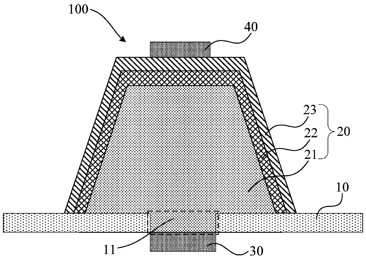
Image

Examples
Embodiment Construction
[0060] The technical solutions of the present invention will be further described below in conjunction with the accompanying drawings and through specific implementation methods. It should be understood that the specific embodiments described here are only used to explain the present invention, but not to limit the present invention. In addition, it should be noted that, for the convenience of description, only some structures related to the present invention are shown in the drawings but not all structures.
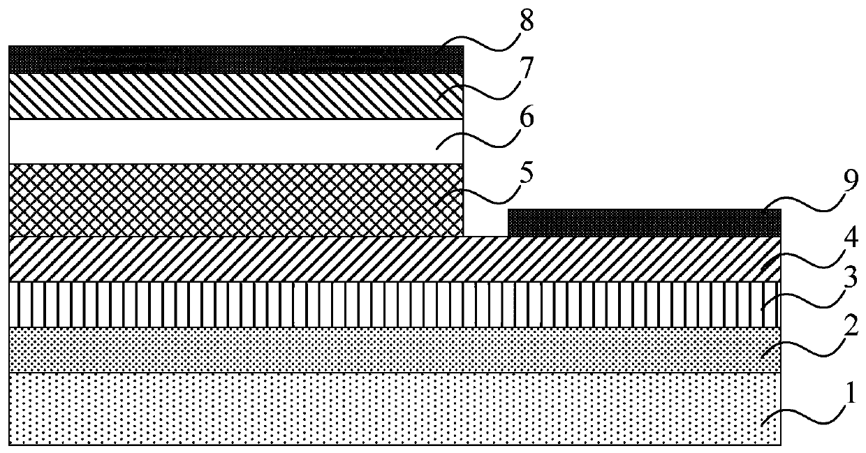
[0061] figure 1 is a schematic diagram of a micro-LED structure in the prior art, such as figure 1 As shown, the micro LED structure includes a substrate 1, a nucleation layer 2, a non-doped GaN layer 3, an n-type GaN layer 4, a multi-quantum well layer 5, an electron blocking layer 6 and a p-type GaN layer 7 stacked in sequence, Among them, part of the multi-quantum well layer 5, the electron blocking layer 6 and the p-type GaN layer 7 are etched away, a p-electrode 8...
PUM
| Property | Measurement | Unit |
|---|---|---|
| Thickness | aaaaa | aaaaa |
Abstract
Description
Claims
Application Information