Modeling method for forming and positioning internal defects of three-dimensional photonic crystal

A technology of photonic crystals and internal defects, applied in special data processing applications, instruments, electrical digital data processing, etc., can solve problems that restrict the performance of three-dimensional photonic crystal devices and poor compatibility

Active Publication Date: 2019-07-12
HANGZHOU DIANZI UNIV
View PDF6 Cites 5 Cited by
  • Summary
  • Abstract
  • Description
  • Claims
  • Application Information

AI Technical Summary

Problems solved by technology

[0002] In the absence of external force, limited by the material itself and processing technical conditions, when the internal structure of the three-dimensional photonic crystal is formed, its forming position has a certain degree of randomness. As a result, the compatibility of the molding structure with the device is poor, which in turn restricts the performance of the three-dimensional photonic crystal device

Method used


Image

  • Modeling method for forming and positioning internal defects of three-dimensional photonic crystal
  • Modeling method for forming and positioning internal defects of three-dimensional photonic crystal
  • Modeling method for forming and positioning internal defects of three-dimensional photonic crystal

Examples


Embodiment Construction

[0041] In order to illustrate the embodiments of the present invention more clearly, the specific implementation manners of the present invention will be described below with reference to the accompanying drawings. Obviously, the accompanying drawings in the following description are only some embodiments of the present invention, and those skilled in the art can obtain other accompanying drawings based on these drawings and obtain other implementations.

[0042] The modeling method for forming and locating internal defects in a three-dimensional photonic crystal according to an embodiment of the present invention specifically includes the following steps:

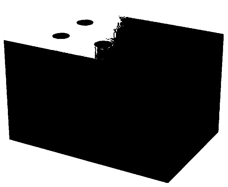
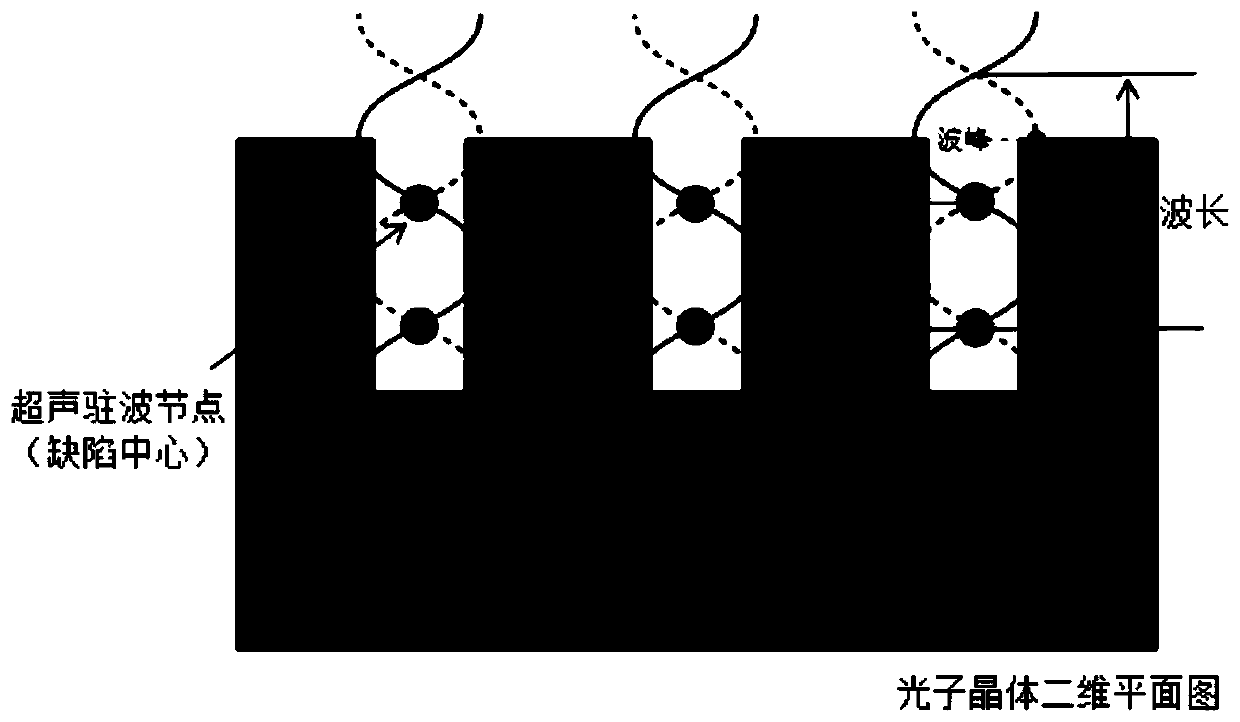
[0043] Step 1: If figure 1 As shown, the basic parameters for designing a two-dimensional array of cylindrical holes include: hole diameter D, hole depth H, and hole distance D s ;Adjust the parameter variables of the external ultrasonic wave, including: the emission speed c of the ultrasonic wave 0 , the emission frequ...


PUM


Abstract

The invention relates to a modeling method for forming and positioning internal defects of a three-dimensional photonic crystal. The modeling method comprises the following steps: defining size parameters of two-dimensional array cylindrical holes in a silicon-based three-dimensional photonic crystal; adjusting the parameter variable of the ultrasonic wave to position the center position of the internal defect of the silicon-based three-dimensional photonic crystal; establishing an ultrasonic temperature field mathematical model equation; and according to the size parameters of the two-dimensional array cylindrical holes, adjusting the ultrasonic length to control the directional movement of silicon-based atoms, and based on an ultrasonic temperature field mathematical model equation, controlling the forming of silicon-based internal defects. The directional movement mechanism of acoustic radiation force to silicon-based atoms is utilized; based on the phase field model, the magnitudeof acoustic radiation force is changed to control positioning of internal defects; an ultrasonic temperature field mathematical model is established, the magnitude of acoustic radiation force is adjusted by changing parameters of external ultrasonic standing waves, the change mechanism of defect positions in the three-dimensional photonic crystals is studied, and a new idea is provided for numerical simulation of the three-dimensional photonic crystals which are periodically and regularly arranged.

Description

technical field [0001] The invention belongs to the technical field of micro-nano manufacturing, and in particular relates to a modeling method for forming and locating internal defects of a three-dimensional photonic crystal. Background technique [0002] In the absence of external force, limited by the material itself and processing technical conditions, when the internal structure of the three-dimensional photonic crystal is formed, its forming position has a certain degree of randomness, which makes the forming structure poorly compatible with the device, which in turn restricts the three-dimensional photonic crystal. device performance. Inspired by the control of the deflection of the microcavity by the sound field, an ultrasonic external force is introduced to couple the sound field with the temperature field. The phase field model is a computational simulation method for simulating and predicting the evolution of material morphology and microstructure at the mesoscop...

Claims


Application Information

Patent Timeline
Patent Type & Authority Applications(China)
IPC IPC(8): G06F17/50
CPCG06F30/20
Inventor 张俐楠朱伟华刘红英陈超吴立群王洪成
Owner HANGZHOU DIANZI UNIV
Why Eureka
Try Eureka