SES production line

A production line and conveying direction technology, applied in the field of SES production line, can solve the problems of weakening the etching reaction and poor etching uniformity on the surface of the PCB board, so as to reduce the possibility and ensure the uniformity.

Active Publication Date: 2019-07-19
CIRCUIT TECH MACHINERY
View PDF6 Cites 11 Cited by
  • Summary
  • Abstract
  • Description
  • Claims
  • Application Information

AI Technical Summary

Problems solved by technology

[0002] The SES production line is an important link in the production process of PCB boards. It mainly includes film stripping, etching, and tin stripping. The film used for anti-plating purposes is stripped with water through film stripping, and the copper in the non-conductor part is sprayed with water through etching. Water corrosion method removes the tin layer used for anti-etching effect by removing tin with water. In the etching process, it is usually achieved by spraying etching solution, but there will be etching solution in the actual spray etching process. Accumulation on the surface of the PCB board leads to the accumulation of liquid, which will directly lead to the weakening of the etching reaction at the accumulation of liquid, making the etching uniformity of the entire PCB board surface poor, which needs further improvement

Method used


Image

  • SES production line
  • SES production line
  • SES production line

Examples


Embodiment Construction

[0042] The present invention will be described in further detail below in conjunction with the accompanying drawings.

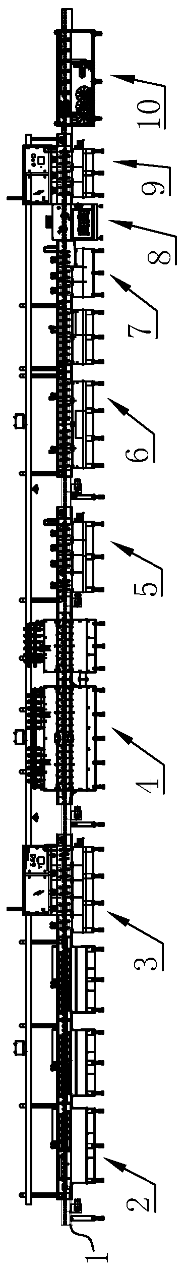
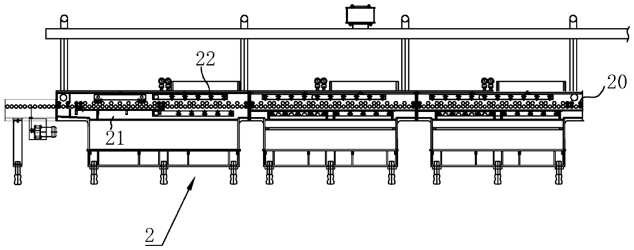
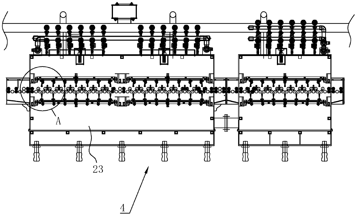
[0043] A PCB board cleaning line, such as figure 1 As shown, it includes a strip-shaped conveying platform 1, and the PCB board is placed on the conveying platform 1 and continuously transported towards it. On the conveying platform 1, a demoulding device, a first water washing device 3, and an etching device are sequentially arranged along the conveying direction. 4. The second water washing device 5, the tin stripping device 6, the third water washing device 7, the grinding plate device 8, the fourth water washing device 9 and the air drying device 10, so that the stripping, etching and tin stripping are completed in sequence during the PCB board transportation process , grinding board and air-drying processing, and the PCB board output from the end of the conveyor table 1 is in a dry state and can directly proceed to the next production process, which effe...


PUM


Abstract

The invention discloses an SES production line. The SES production line comprises a conveying table, a demoulding device, an etching device and a solder stripping device, wherein the demoulding device, the etching device and the solder stripping device are sequentially arranged in the conveying direction; the etching device comprises a vacuum etching chamber; first spraying heads used for sprayingan etching liquid is arranged in the vacuum etching chamber; the first spraying heads are located on the upper side and the lower side of a PCB respectively and are arranged at intervals in the conveying direction; a liquid sucking head used for sucking the etching liquid accumulated on the upper surface of the PCB is arranged between the adjacent first spraying heads in the conveying direction,so that the PCB is continuously conveyed forwrads on the conveying table, and the processing of demoulding, etching and solder stripping is gradually realized; and the etching liquid is sprayed to thesurface of the PCB from the upper side and the lower side through the first spraying heads in the etching process, and the etching liquid accumulated on the upper surface of the PCB is sucked away under the action of a suction force of the liquid suction head, so that the situation that an etching reaction is weakened due to the accumulated liquid on the upper surface of the PCB is effectively avoided, and the purpose of more uniform etching is achieved.

Description

technical field [0001] The invention relates to the field of PCB board production, more specifically, it relates to a SES production line. Background technique [0002] The SES production line is an important link in the production process of PCB boards. It mainly includes film stripping, etching, and tin stripping. The film used for anti-plating purposes is stripped with water through film stripping, and the copper in the non-conductor part is sprayed with water through etching. Water corrosion method removes the tin layer used for anti-etching effect by removing tin with water. In the etching process, it is usually achieved by spraying etching solution, but there will be etching solution in the actual spray etching process. Accumulation on the surface of the PCB board leads to the accumulation of liquid, which will directly lead to the weakening of the etching reaction at the accumulation of liquid, making the etching uniformity of the entire PCB board surface poor, which ...

Claims


Application Information

Patent Timeline
Patent Type & Authority Applications(China)
IPC IPC(8): H05K3/06
CPCH05K3/068H05K2203/075
Inventor 任春花白胜辉
Owner CIRCUIT TECH MACHINERY
Why Eureka
Try Eureka