Check patentability & draft patents in minutes with Patsnap Eureka AI!

SOI-based SiGe double-heterojunction photosensitive transistor detector

A photosensitive transistor and double heterojunction technology, applied in semiconductor devices, electrical components, circuits, etc., can solve the problems of increased transit time of photogenerated carriers, reduced device operating speed, and poor frequency characteristics

Inactive Publication Date: 2019-07-23
BEIJING UNIV OF TECH
View PDF2 Cites 5 Cited by
  • Summary
  • Abstract
  • Description
  • Claims
  • Application Information

AI Technical Summary

Problems solved by technology

In 2013, Taiwan reported a SiGe / Si HPT detector based on a 0.18μm BiCMOS process, which achieved a responsivity of up to 75A / W for light absorption at 750nm. However, due to the use of photogenerated carriers in the substrate, its frequency characteristics Poor, slow device operation
It can be seen that the responsivity and response speed of the current vertical structure Si-based photodetector still need to be improved, and there is a contradiction in the optimization of the responsivity and working speed of the phototransistor. To obtain a high responsivity, it is necessary to increase the thickness of the absorption region Improve the absorption efficiency of light, but this will increase the transit time of photo-generated carriers, thereby reducing the working speed of the device, and the influence of photo-generated carriers in the substrate is also a factor that cannot be ignored

Method used


Image

  • SOI-based SiGe double-heterojunction photosensitive transistor detector
  • SOI-based SiGe double-heterojunction photosensitive transistor detector
  • SOI-based SiGe double-heterojunction photosensitive transistor detector

Examples


Embodiment Construction

[0021] In order to make the purpose, technical solution and advantages of the present invention clearer, the present invention will be further described in detail below in conjunction with specific embodiments and with reference to the accompanying drawings.

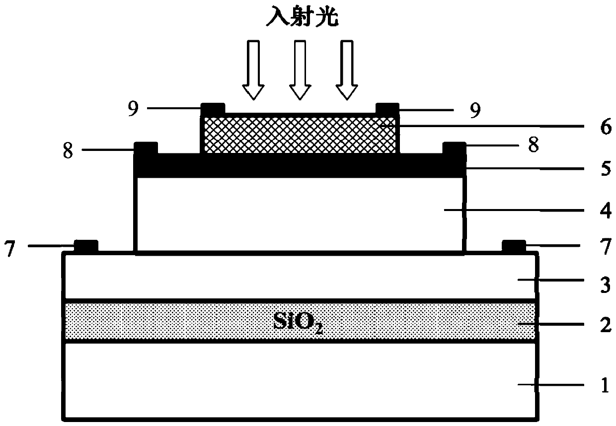
[0022] Such as figure 1 As shown, the embodiment of the present invention provides SOI-based SiGe double heterojunction phototransistor detectors including:

[0023] An SOI substrate, including the underlying Si(1) and SiO 2 (2) insulating layer; a Si sub-collector region (3), a Si collector region (4), a SiGe base region (5) and a polycrystalline Si emitter region (6) are sequentially prepared on the SOI substrate ; The optical window of the detector is located in the polycrystalline Si emission area; the collector (7) is made on the Si sub-collector; the base (8) is made on the SiGe base region; the emitter (9) is made on the polycrystalline On the Si emitter;

[0024] Wherein the lower layer Si(1) in the SOI substr...


PUM

PropertyMeasurementUnit
Thicknessaaaaaaaaaa

Abstract

The invention discloses an SOI-based SiGe double-heterojunction photosensitive transistor detector. An SOI substrate is adopted to replace a Si substrate. The detector comprises an SOI substrate whichis composed of a lower Si layer and a SiO2 layer. A Si secondary collector region, a Si collector region, a SiGe base region and a polycrystalline Si emitter region are sequentially prepared on the SOI substrate. Due to the refractive index difference generated by different refractive indexes of the Si material and the SiO2 material, a reflecting mirror can be formed on the Si / SiO2 interface, incident light can be reflected and absorbed again after reaching the Si / SiO2 interface in the SOI substrate, and the absorption efficiency is improved; in addition, due to the existence of the SiO2 layer in the SOI substrate, slow carriers generated in the lower Si layer of the substrate can be isolated, and the parasitic capacitance of the device is reduced, so that the working speed is increased.The photoelectric detector is manufactured on the SOI substrate, so that high-speed and high-efficiency optical detection can be realized.

Description

technical field [0001] The present invention relates to the technical field of semiconductor optoelectronics, in particular to an SOI-based SiGe double heterojunction phototransistor detector (HPT) that takes into account both responsivity and response speed, which can relieve the light absorption efficiency and The contradiction between working speed, while achieving high-speed and efficient light detection. Background technique [0002] The rapid development of modern optical communication requires that the optical communication network must have greater information transmission capacity and faster information processing speed, and the requirements for integrated circuit integration are getting higher and higher. Traditional electrical interconnection technology has become the bottleneck of high-speed data communication. . Optical interconnection technology has become a key technology to be solved urgently. Therefore, silicon-based photonic technologies suitable for opti...

Claims


Application Information

Patent Timeline
IPC IPC(8): H01L31/11H01L31/0232H01L31/0352H01L31/0392
CPCH01L31/02327H01L31/035272H01L31/03921H01L31/1105
Inventor 谢红云刘先程沙印郭敏马佩张万荣
Owner BEIJING UNIV OF TECH
Features
  • R&D
  • Intellectual Property
  • Life Sciences
  • Materials
  • Tech Scout
  • Unparalleled Data Quality
  • Higher Quality Content
  • 60% Fewer Hallucinations
Learn More