Display device using semiconductor light emitting element

A technology for display devices and light-emitting elements, applied in semiconductor devices, identification devices, lighting devices, etc., can solve the problems of weak resistance to external impact, size and ratio limitations, image quality limitations, etc., to reduce physical impact and achieve uniform supply paths. , the effect of increasing the degree of freedom of design

Active Publication Date: 2019-07-23
LG ELECTRONICS INC
View PDF10 Cites 5 Cited by
  • Summary
  • Abstract
  • Description
  • Claims
  • Application Information

AI Technical Summary

Problems solved by technology

[0004] However, due to the shape of the semiconductor light emitting element, the size and ratio of the p-electrode and n-electrode are limited, which may lead to limitations in the improvement of image quality
In addition, the semiconductor light-emitting element has a disadvantage in that it is weak in resistance to external impact due to its low thickness compared to its area.

Method used


Image

  • Display device using semiconductor light emitting element
  • Display device using semiconductor light emitting element
  • Display device using semiconductor light emitting element

Examples


Embodiment Construction

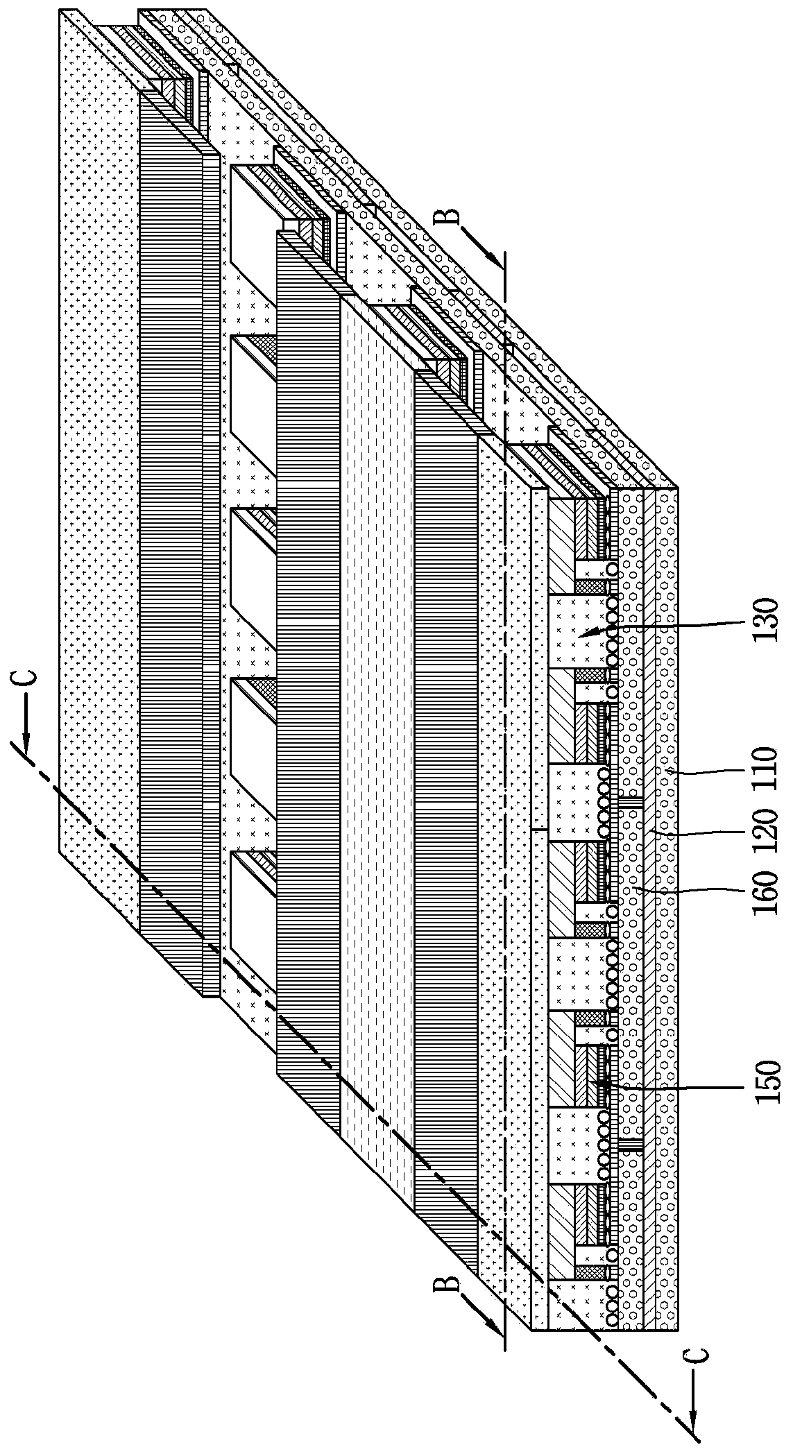
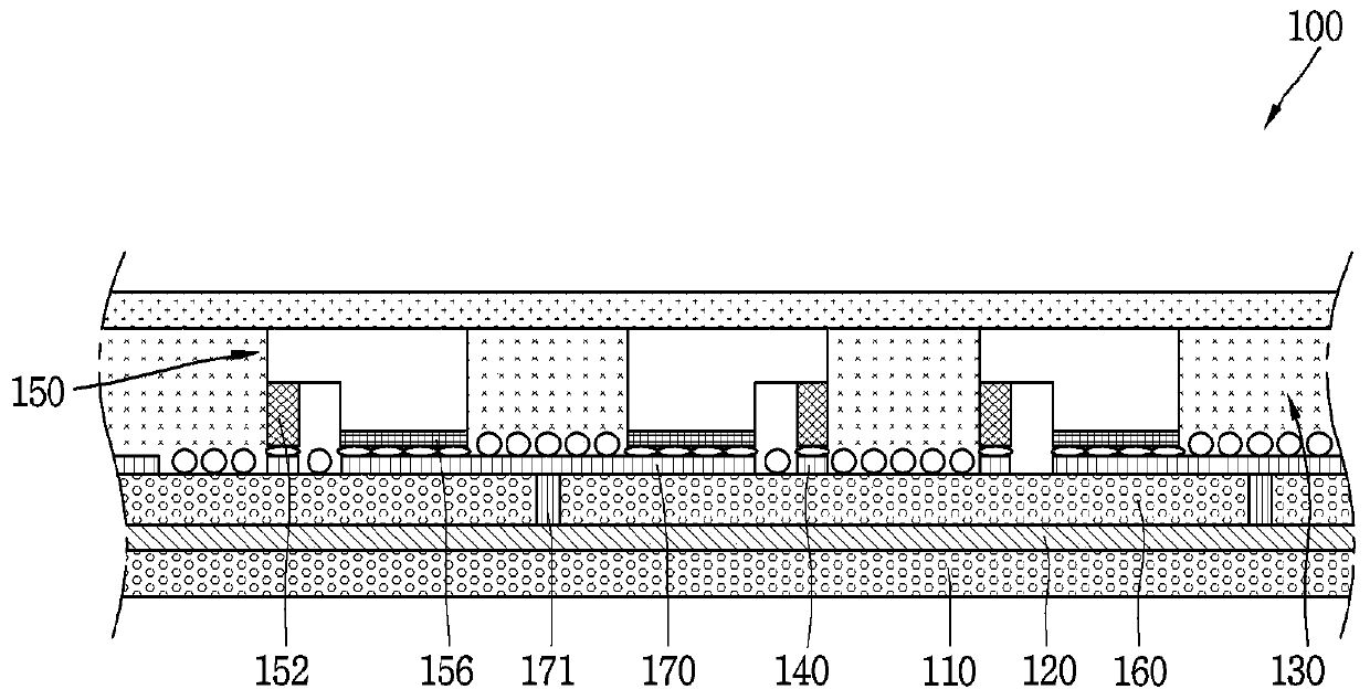
[0037] Hereinafter, embodiments disclosed herein will be described in detail with reference to the accompanying drawings, the same or similar elements will be denoted by the same reference numerals regardless of the numbers in the drawings, and redundant descriptions thereof will be omitted. The suffixes "module" and "unit" used for constituent elements disclosed in the following description are only intended to facilitate description of the specification, and the suffixes themselves do not give any special meaning or function. In addition, in describing the embodiments disclosed herein, when it is judged that a detailed description of known technology related to the present invention obscures the gist of the present disclosure, the detailed description will be omitted. In addition, it should be noted that the accompanying drawings are only shown to easily explain the concept of the present invention, and thus, it should not be construed as limiting the technical concept disclo...


PUM


Abstract

The present invention relates to a display device and, particularly, to a display device using a semiconductor light emitting element. The display device according to the present invention comprises aplurality of semiconductor light emitting elements mounted on a substrate, wherein at least one of the semiconductor light emitting elements comprises: a first conductive electrode and a second conductive electrode; a first conductive semiconductor layer in which the first conductive electrode is disposed; a second conductive semiconductor layer which overlaps the first conductive semiconductor layer and in which the second conductive electrode is disposed; a first passivation layer formed to cover outer surfaces of the first conductive semiconductor layer and the second conductive semiconductor layer; and a second passivation layer formed to cover the first passivation layer and formed such that at least a portion thereof varies in thickness.

Description

technical field [0001] The present disclosure relates to a display device and a method of manufacturing the same, and more particularly, to a display device using a semiconductor light emitting element. Background technique [0002] In recent years, display devices having excellent characteristics such as low profile, flexibility, and the like have been developed in the field of display technology. In contrast, representatives of the main displays commercialized today are liquid crystal displays (LCDs) and active matrix organic light emitting diodes (AMOLEDs). However, there are problems such as not so fast response time, difficulty in achieving flexibility in the case of LCD, and disadvantages such as short lifetime, not so good yield, and low flexibility in the case of AMOLED. [0003] On the other hand, light-emitting diodes (LEDs) are well-known light-emitting devices for converting electric current into light, and since red LEDs using GaAsP compound semiconductors were...

Claims


Application Information

Patent Timeline
Patent Type & Authority Applications(China)
IPC IPC(8): H05B33/12H05B33/10H01L27/15G09F9/30H01L33/36
CPCH01L27/15H01L33/36H05B33/10H05B33/12G09F9/30H01L33/62H01L33/46H01L33/486H01L25/0753H01L33/52H01L27/156G09F9/301H01L2924/12041H01L33/38H01L33/44
Inventor 崔桓准李勇翰
Owner LG ELECTRONICS INC
Why Eureka
Try Eureka