
Semiconductor device having body contacts with dielectric spacers and corresponding methods of manufacture

A semiconductor and spacer technology, applied in semiconductor/solid-state device manufacturing, semiconductor devices, electric solid-state devices, etc., can solve problems such as increasing the quality factor of the total gate charge

Pending Publication Date: 2019-07-30
INFINEON TECH AUSTRIA AG
View PDF0 Cites 2 Cited by
  • Summary
  • Abstract
  • Description
  • Claims
  • Application Information

AI Technical Summary

Problems solved by technology

However, smaller gate capacitance increases the overall gate charge figure of merit (FOMg)

Method used


Image

  • Semiconductor device having body contacts with dielectric spacers and corresponding methods of manufacture
  • Semiconductor device having body contacts with dielectric spacers and corresponding methods of manufacture
  • Semiconductor device having body contacts with dielectric spacers and corresponding methods of manufacture

Examples


Embodiment Construction

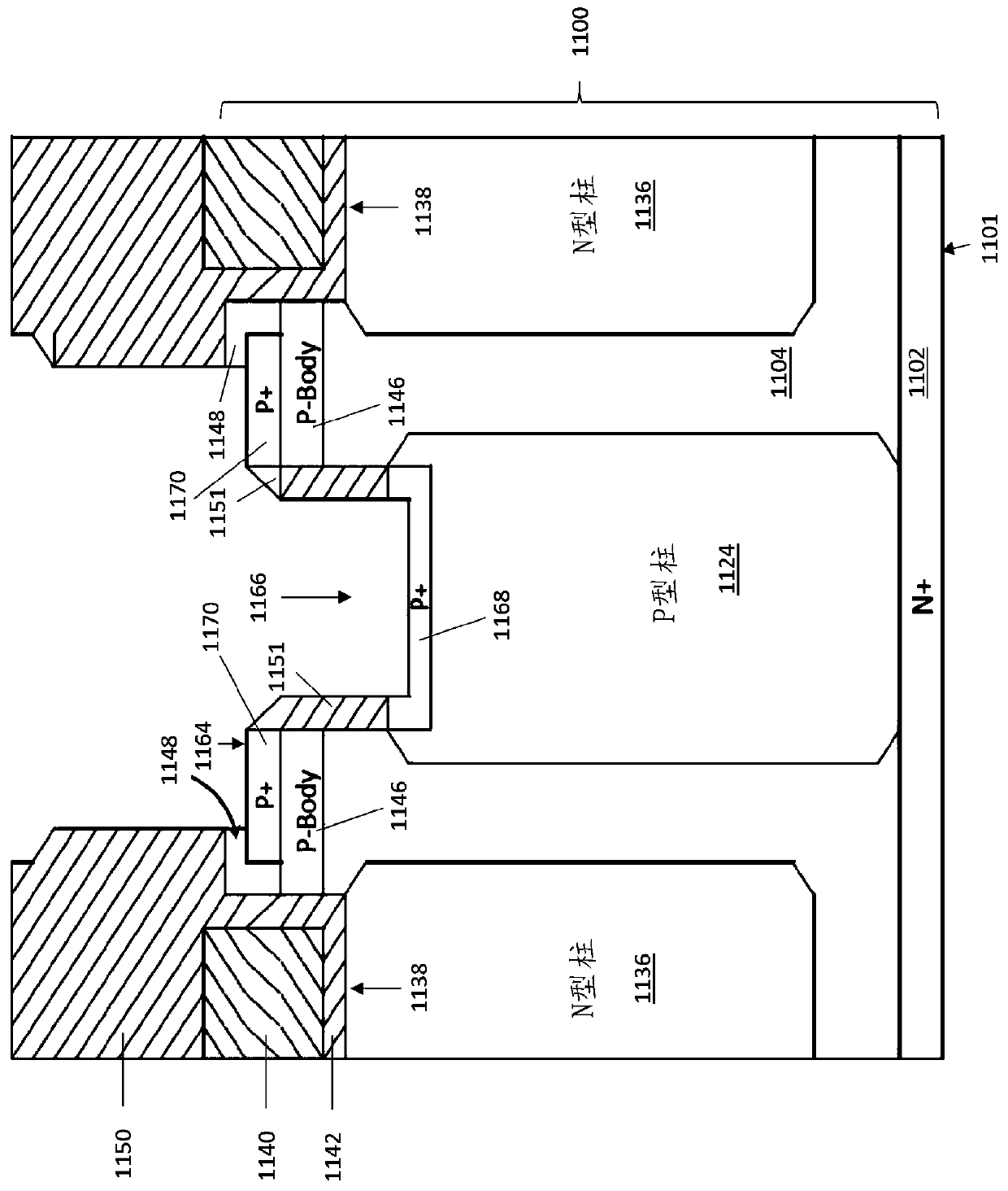
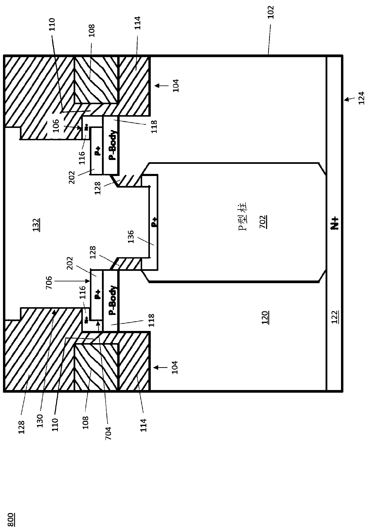
[0014] The embodiments described herein provide a power MOSFET with a reduced channel size and a good FOMg, and a corresponding manufacturing method. By introducing a spacer dielectric along the sidewall of the contact to the highly doped body contact region of the power device, the lateral dimension of the channel region can be further reduced, while the source capacitance is reduced and the highly doped body contact region and the trench are increased. The distance between road areas. The small fin-shaped part of the device body region between the contact opening / groove and the gate trench in the semiconductor substrate is connected in parallel with the contact opening / groove, thereby reducing the IV curve and DIBL (drain induced barrier drop) )swing. The highly doped body contact region is decoupled from the channel region by dielectric along the spacers of the contact opening / groove, thereby improving threshold voltage stability. The dielectric spacer also introduces stre...


PUM


Abstract

The present invention discloses a semiconductor device having body contacts with dielectric spacers and corresponding methods of manufacture. The semiconductor device includes a trench extending intoa first main surface of a semiconductor substrate, and a gate electrode and a gate dielectric in the trench. The gate dielectric separates the gate electrode from the semiconductor substrate. A firstregion having a first conductivity type is formed in the semiconductor substrate at the first surface adjacent the trench. A second region having a second conductivity type is formed in the semiconductor substrate below the first region adjacent the trench. A third region having the first conductivity type is formed in the semiconductor substrate below the second region adjacent the trench. A contact opening in the semiconductor substrate extends into the second region. An electrically insulative spacer is disposed on sidewalls of the semiconductor substrate formed by the contact opening, andan electrically conductive material in the contact opening adjoins the electrically insulative spacer on the sidewalls.

Description

Technical field [0001] The present invention relates to a semiconductor device having a body contact and a dielectric spacer and a corresponding manufacturing method. Background technique [0002] The channel size of the power MOSFET is routinely reduced to increase performance. The distance between the channel of the device and the groove contact of the body region of the device has also become smaller, resulting in several key trade-offs, including: the mutual p+ contact implant into the groove and the channel dopant Effect; and when the depletion capacitance reduces the gate control and the parasitic source capacitance increases, the slope of the threshold voltage characteristic decreases. [0003] The distance between the channel and groove contacts can be kept large enough, but this results in a higher Rdson (on-state resistance). The decrease in the slope of the threshold voltage characteristic can be solved by using a thinner oxide that produces a smaller gate capacitance....

Claims


Application Information

Patent Timeline
IPC IPC(8): H01L29/10H01L29/423H01L27/06H01L21/336
CPCH01L29/7827H01L29/1033H01L29/4236H01L29/66666H01L27/0629H01L29/407H01L29/41766H01L29/66719H01L29/66727H01L29/66734H01L29/7806H01L29/7813H01L29/7843H01L29/0634H01L29/0869H01L29/1095H01L21/76805H01L21/76831H01L29/41741H01L29/423H01L29/6634H01L29/66348H01L29/7397H01L29/872
Inventor 黄伟峻T.法伊尔M.珀尔兹尔M.勒施
Owner INFINEON TECH AUSTRIA AG
Learn More