Display panel and manufacturing method

A technology for a display panel and a manufacturing method, which is applied in the manufacture of semiconductor/solid-state devices, electrical components, and electrical solid-state devices, etc., can solve problems such as poor brightness uniformity of OLED display panels, and achieve the advantages of improving uniformity, increasing potential, and reducing voltage drop. Effect

Inactive Publication Date: 2019-07-30
SHENZHEN CHINA STAR OPTOELECTRONICS SEMICON DISPLAY TECH CO LTD
View PDF8 Cites 30 Cited by
  • Summary
  • Abstract
  • Description
  • Claims
  • Application Information

AI Technical Summary

Problems solved by technology

[0005] The present application provides a display panel and a manufacturing method to solve the technical problem of poor brightness uniformity of existing OLED display panels

Method used


Image

  • Display panel and manufacturing method
  • Display panel and manufacturing method
  • Display panel and manufacturing method

Examples


Embodiment Construction

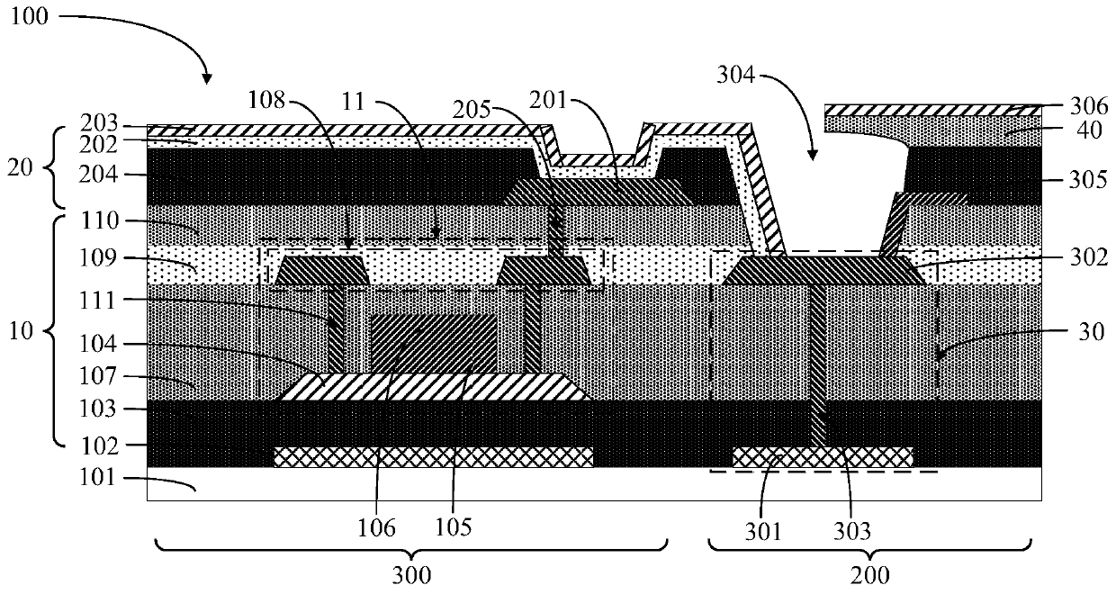
[0062] The following descriptions of the various embodiments refer to the accompanying drawings to illustrate specific embodiments that the present application can be used to implement. The directional terms mentioned in this application, such as [top], [bottom], [front], [back], [left], [right], [inside], [outside], [side], etc., are for reference only The orientation of the attached schema. Therefore, the directional terms used are used to illustrate and understand the application, but not to limit the application. In the figures, structurally similar elements are denoted by the same reference numerals.

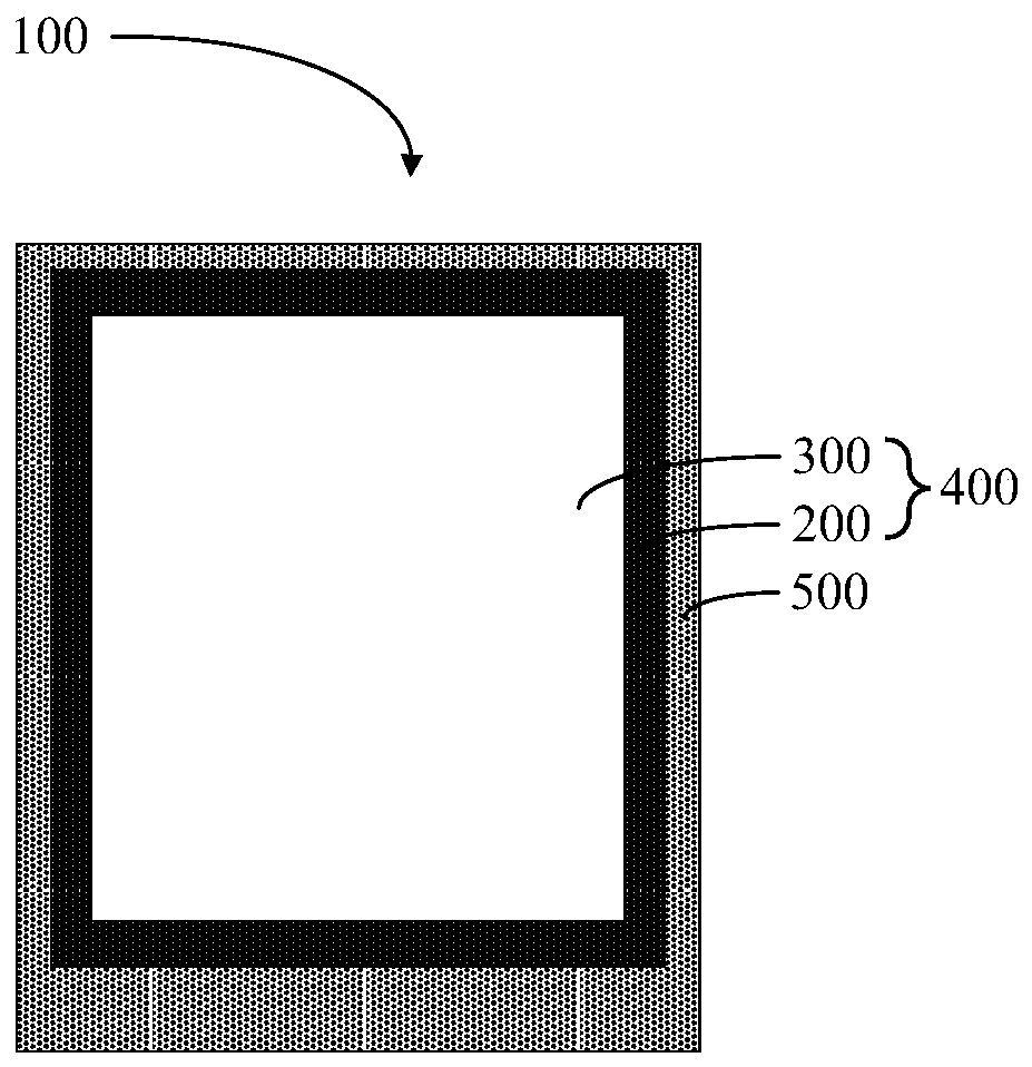
[0063] see figure 1 , figure 1 It is a plane structure diagram of the display panel 100 of the present application.

[0064] The display panel 100 includes a display area 400 and a non-display area 500 located around the display area 400 . The display area 400 includes a first area 200 located at the edge of the display area 400 and a second area 300 surrounded by the ...


PUM


Abstract

The invention provides a display panel and a manufacturing method thereof, wherein a display area of the display panel comprises a first area positioned at the edge of the display area; and an auxiliary electrode and a light-emitting protection layer positioned on the auxiliary electrode are arranged in the first area, and orthographic projection of the light-emitting protection layer on the auxiliary electrode is partially overlapped with the auxiliary electrode. According to the invention, an auxiliary electrode is arranged in the edge area of a display panel, and cathode layer is in lap joint with the auxiliary electrode, so that the potential of the cathode layer is increased, the voltage drop of the cathode layer is slowed down, and the brightness uniformity of the display panel is improved.

Description

technical field [0001] The present application relates to the display field, in particular to a display panel and a manufacturing method. Background technique [0002] In flat panel display technology, Organic Light-Emitting Diode (OLED) display has many advantages such as thinness, active light emission, fast response speed, large viewing angle, wide color gamut, high brightness and low power consumption, etc., and has gradually become the successor. The third generation display technology after liquid crystal display. [0003] As the size of the display panel increases, the area of ​​the cathode layer of the OLED also increases. The transmittance of the cathode layer of the top-emitting OLED display requires that the cathode should not be too thick. Such a large-area cathode layer will inevitably lead to a decrease in the in-plane voltage, resulting in a decrease in the brightness of the screen and poor brightness uniformity. [0004] Therefore, there is an urgent need f...

Claims


Application Information

Patent Timeline
Patent Type & Authority Applications(China)
IPC IPC(8): H01L51/52H01L27/32H01L51/56
CPCH10K59/12H10K50/824H10K59/1201H10K71/00
Inventor 范英春
Owner SHENZHEN CHINA STAR OPTOELECTRONICS SEMICON DISPLAY TECH CO LTD
Why Eureka
Try Eureka