Directional emission organic semiconductor light emitting diode array based on metal nano electrodes and preparation thereof

A technology of electroluminescent devices and organic semiconductors, which is applied in the field of OLED arrays, can solve the problems of insufficient attention to the emission directionality of the device, and the failure to obtain optimization effects, etc., and achieve good directional emission characteristics, improved light extraction efficiency, and low cost.

Pending Publication Date: 2019-08-02
BEIJING UNIV OF TECH
View PDF0 Cites 2 Cited by
  • Summary
  • Abstract
  • Description
  • Claims
  • Application Information

AI Technical Summary

Problems solved by technology

However, these devices still use a flat "sandwich" structure, and have not achieved ideal optimization results
At present, most of the research on OLED devices is efficiency, chromaticity and color stability, etc., and the emission directionality of the device has not received enough attention.

Method used


Image

  • Directional emission organic semiconductor light emitting diode array based on metal nano electrodes and preparation thereof
  • Directional emission organic semiconductor light emitting diode array based on metal nano electrodes and preparation thereof
  • Directional emission organic semiconductor light emitting diode array based on metal nano electrodes and preparation thereof

Examples


Embodiment 1

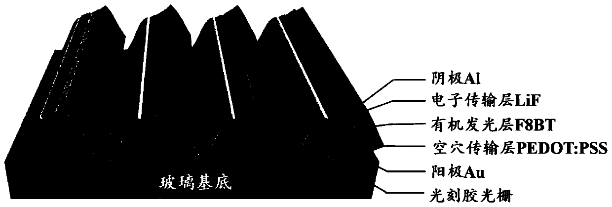
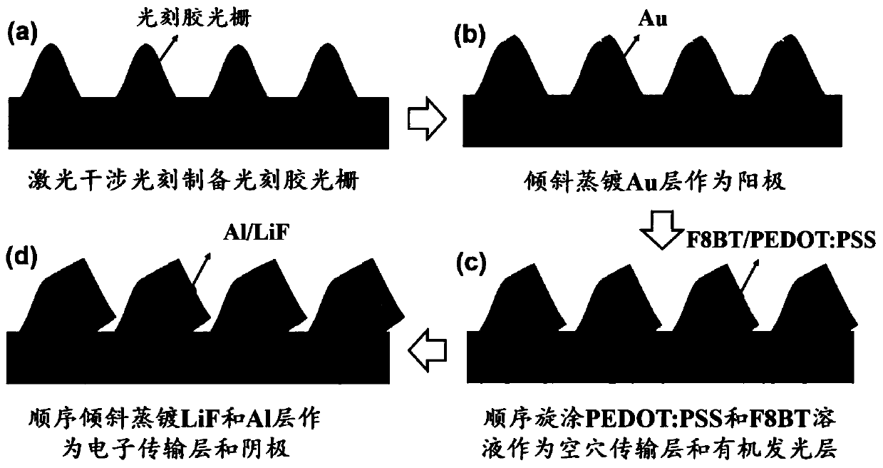
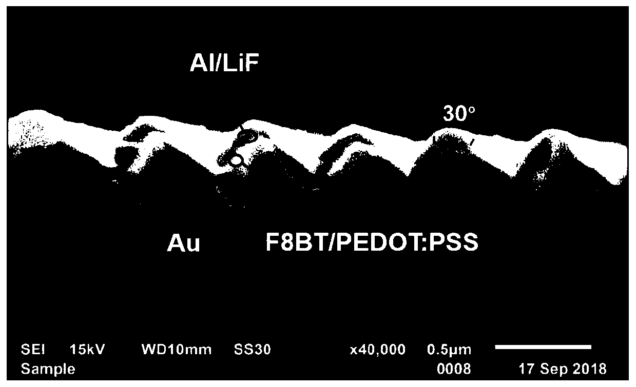
[0022] (1), the selected size is 2×2cm 2 The glass is used as the substrate, and after repeated cleaning, it is etched with high-power oxygen plasma for 5-10 minutes to completely remove the organic matter on the substrate. Then, spin-coat S1805 photoresist on the substrate at a rotational speed of 3000 rpm for 30 seconds. Prepare a photoresist film with a thickness of about 200 nm. The samples were then placed on a heating plate and heated at 110 °C for 90 s. Then use the 343nm laser interference optical path to expose the sample, and after development, a photoresist grating structure with a period of 500nm and a modulation depth of about 180nm can be obtained, such as figure 2 (a).

[0023] (2) The grid line of the photoresist grating is used as the template for preparing the nanoscale organic electroluminescent device. Deposit an Au layer on one side of the grating as an anode using oblique evaporation technology, such as figure 2 (b). The thickness of the Au thin f...


PUM


Abstract

The invention relates to a directional emission organic semiconductor light emitting diode array based on metal nano electrodes and preparation thereof, and belongs to the technical field organic optoelectronics and nanophotonics. On a glass substrate, a photoresist nano grating is utilized to serve as a template, nano-scale organic light emitting diodes parallel to the located inclined planes areprepared on the inclined planes at the same side of each convex grid line of the nano grating, and the nano-scale organic light emitting diode includes an anode layer Au, a hole transport layer PEDOT: PSS, an organic light emitting layer F8BT film, an electron transport layer LiF and a cathode Al which are sequentially laminated outward from the side surface of the convex grid line. The inclinedorganic light emitting diodes are formed on the nano grating structure, and all of the organic light emitting diodes form an array structure. The device achieves the working mode of end emission and obtains the directional emission nano OLED (Organic Light Emitting Diode) array.

Description

technical field [0001] The invention belongs to the technical fields of organic optoelectronics and nanophotonics, and proposes a design idea of ​​a nanoscale organic semiconductor electroluminescent device (OLED), realizes its end emission working mode, and obtains an OLED array with directional output. Background technique [0002] Organic light emitting diodes (OLEDs) have a series of characteristics such as wide viewing angle, light weight, suitable for flexible substrates, and simple process, and have great application prospects in the fields of new displays and solid-state lighting. The light coupling output efficiency or output light extraction efficiency of a typical organic electroluminescent device with a "sandwich" flat plate structure on a transparent substrate is only about 20%, and 80% of the light is confined inside the device or lost during transmission. By introducing micro-nano structures into the active layer, electrode layer or even the substrate of the d...

Claims


Application Information

Patent Timeline
Patent Type & Authority Applications(China)
IPC IPC(8): H01L51/52H01L51/56
CPCH10K50/85H10K71/00
Inventor 张新平黄翠莺
Owner BEIJING UNIV OF TECH
Why Eureka
Try Eureka