

Microstrip coupler and PCB (printed circuit board)
A microstrip coupler and etching layer technology, which is applied in the electronic field, can solve the problems of increasing the production cost of the microstrip coupler, and achieve the effects of increasing the coupling strength, reducing the production cost, and widening the distance
- Summary
- Abstract
- Description
- Claims
- Application Information
AI Technical Summary
Problems solved by technology
Method used
Image

Examples
Embodiment Construction
[0017] The following will clearly and completely describe the technical solutions in the embodiments of the present invention with reference to the accompanying drawings in the embodiments of the present invention. Obviously, the described embodiments are some of the embodiments of the present invention, but not all of them. Based on the embodiments of the present invention, all other embodiments obtained by persons of ordinary skill in the art without making creative efforts belong to the protection scope of the present invention.
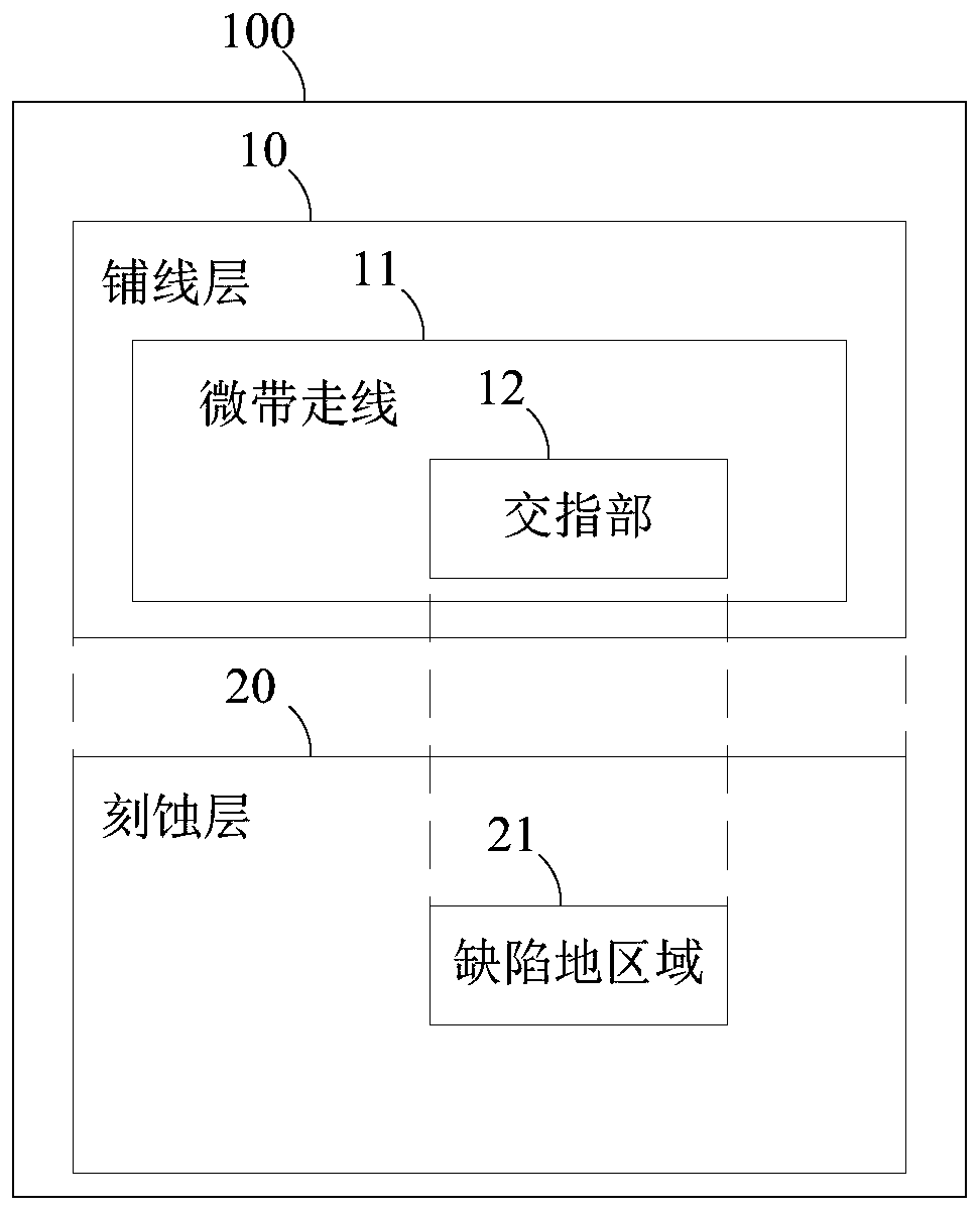
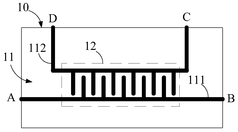
[0018] See figure 1 , figure 1 It is a schematic structural diagram of a microstrip coupler provided by an embodiment of the present invention. For convenience of description, only the parts related to the embodiment of the present invention are shown.
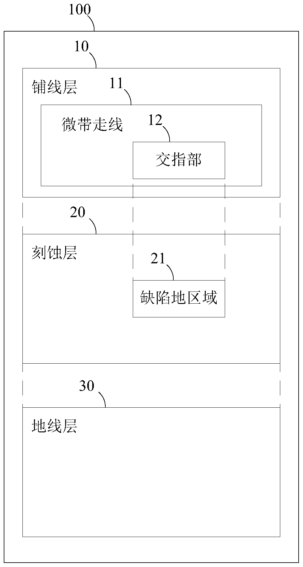
[0019] Such as figure 1 As shown, a microstrip coupler 100 includes: correspondingly laminated wiring layer 10 and etching layer 20 . specifically:
[0020] The wiring layer 10 is used for lay...
PUM
 Abstract
Description
Claims
Application Information