Device and method for testing performance of semiconductor chip

A chip performance, semiconductor technology, applied in the field of communication, can solve the problems of uncontrollable pressure, inapplicability, chip damage, etc., to achieve the effects of low device cost, high operating efficiency, and simple operation

Pending Publication Date: 2019-08-13
SUZHOU TFC OPTICAL COMM CO LTD
View PDF0 Cites 8 Cited by
  • Summary
  • Abstract
  • Description
  • Claims
  • Application Information

AI Technical Summary

Problems solved by technology

[0003] At present, there are mainly two methods for chip performance testing. One is to use POGO-PIN probes, that is, there are spring devices inside the probes, which can be freely retracted. The disadvantage is that this type of probe is not suitable for micron-level PAD spacing, and the spacing between two pins side by side cannot be smaller than the diameter of the probe seat. The smallest available on the market is about 200um.
There is also a hard probe test method. The tip of the hard probe is specially ground to make the tip reach 2-10um level. Although this method can cope with micron-scale spacing chips, it is easy to cause damage to the metal layer of the chip PAD when used. , because it is a rigid contact, the pressure cannot be controlled, and there are often pinhole marks on the PAD. Another point is that after this type of probe is used for a long time, it is very easy to cause the tip of the needle to bend and deform. If it is used again, it will cause permanent damage to the chip. damage

Method used


Image

  • Device and method for testing performance of semiconductor chip
  • Device and method for testing performance of semiconductor chip
  • Device and method for testing performance of semiconductor chip

Examples


Embodiment Construction

[0029] The present invention is described in further detail now in conjunction with accompanying drawing. These drawings are all simplified schematic diagrams, which only illustrate the basic structure of the present invention in a schematic manner, so they only show the configurations related to the present invention.

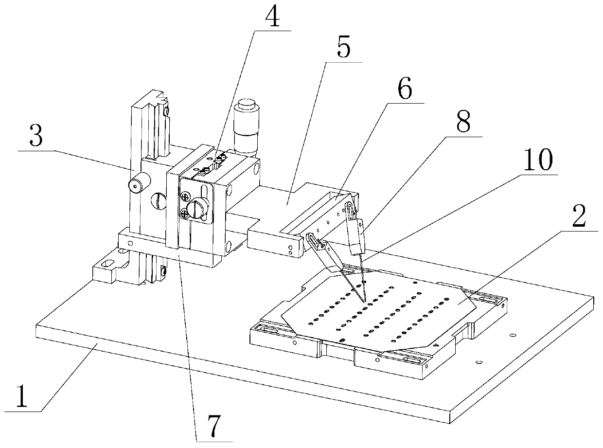
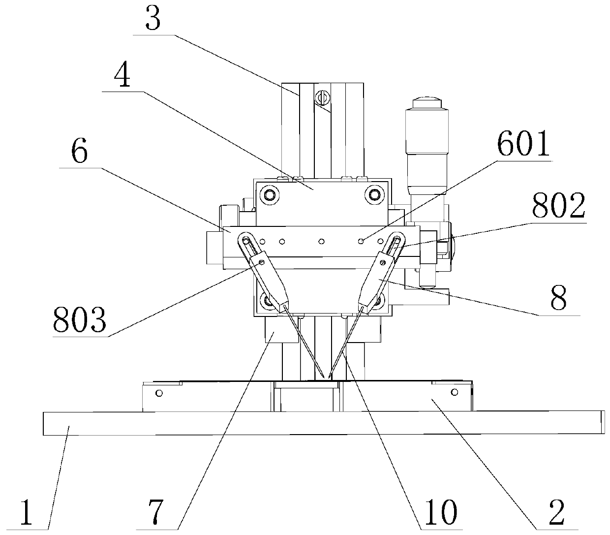
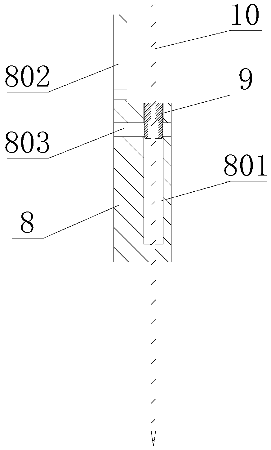
[0030] like Figure 1-2 As shown, a device for performance testing of semiconductor chips includes a base plate 1, an adjustment assembly, a probe assembly and a carrier plate 2. The adjustment assembly and the carrier plate 2 are respectively arranged on the left and right sides of the base plate 1, and the probe assembly is arranged Above the carrier plate 2, the probe assembly is detachably connected to the adjustment assembly;

[0031] The adjustment assembly includes a quick adjustment frame 3, a fine-tuning adjustment frame 4, a mechanical arm 5 and an angle shaft 6, the quick adjustment frame 3 is vertically installed on the base plate 1, and the fine-...


PUM


Abstract

The invention relates to a device for testing the performance of a semiconductor chip. The device comprises a bottom plate, an adjusting assembly, a probe assembly and a carrying disk, wherein the adjusting assembly and the carrying disk are arranged on a left side and a right side of the bottom plate respectively; the adjusting assembly comprises a rapid adjusting frame, a fine tuning adjusting frame, a mechanical arm and an angle shaft; the probe assembly comprises a limiting sleeve, an adjusting sleeve and a tungsten filament probe; the limiting sleeve is detachably connected with the angleshaft; the limiting sleeve is provided with a blind hole; the adjusting sleeve is arranged on the tungsten filament probe in a sleeve manner; the adjusting sleeve is inserted into the blind hole; thetungsten filament probe passes through the limiting sleeve; and a needle head of the tungsten filament probe is positioned below the limiting sleeve. In the device for testing the performance of thesemiconductor chip, a tungsten filament is taken as the probe, so that a large amount of repeated testing can be carried out, and a metal layer of the chip is protected. The extension lengths and distance of two tungsten filament probes can be controlled optionally, and minimum 50[mu]m-grade chip PAD testing can be realized. The device has the advantages of realization of a rapid testing function,easiness in operation, low cost and high operation efficiency.

Description

technical field [0001] The invention relates to the field of communication technology, in particular to a device and method for performance testing of semiconductor chips. Background technique [0002] With the rapid development of the optical communication industry, semiconductor chips play an extremely important role as core components. From data centers, mobile broadband, Internet, national defense and military industries, etc., the application of optical devices is ubiquitous. In order to meet people's different application needs, adapt to In different working environments, the performance reliability of semiconductor chips directly affects the quality, stability and time limit of signal transmission. How to more effectively screen and test semiconductor chips with high performance and higher reliability has become an indispensable part. item of work. [0003] At present, there are mainly two methods for chip performance testing. One is to use POGO-PIN probes, that is, ...

Claims


Application Information

Patent Timeline
Patent Type & Authority Applications(China)
IPC IPC(8): G01R31/26G01R1/073G01R1/02
CPCG01R1/02G01R1/073G01R31/2601
Inventor 邹支农
Owner SUZHOU TFC OPTICAL COMM CO LTD
Why Eureka
Try Eureka