Antenna board and manufacturing method thereof

A manufacturing method and antenna board technology, applied in the direction of antenna, antenna coupling, antenna components, etc., can solve the problems of slow signal transmission, damage to product functions, and inability to weld components, so as to improve production yield and improve anti-interference. the effect of reducing production costs

Active Publication Date: 2019-08-30
SHENZHEN KINWONG ELECTRONICS
View PDF9 Cites 4 Cited by
  • Summary
  • Abstract
  • Description
  • Claims
  • Application Information

AI Technical Summary

Problems solved by technology

[0002] Most of the existing high-frequency antenna boards are double-sided boards, and the signal line (that is, the PCB board used to send and receive antenna signals) is directly designed on the outer layer, resulting in slow signal transmission speed, large loss, and the signal is easily interfered
Put the signal line in the inner layer, and use pp semi-cured adhesive layer for la

Method used


Image

  • Antenna board and manufacturing method thereof
  • Antenna board and manufacturing method thereof
  • Antenna board and manufacturing method thereof

Examples


Embodiment Construction
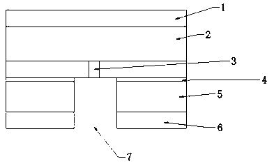
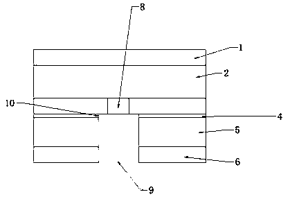
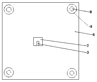
[0036] The most critical idea of ​​the present invention is to place the PCB board for sending and receiving antenna signals between two grounded metal plates, and set a hollow slot on one of the metal plates, so that the antenna signal can only be sent and received through the hollow slot, reducing interference .

[0037] In order to discuss the feasibility of the concept of the present invention, according to the technical content, structural features, achieved goals and effects of the present invention, it will be described in detail in conjunction with the implementation and accompanying drawings.

[0038] see figure 1 , figure 2 as well as image 3 , an antenna board, comprising a grounded first metal plate 1, a PCB board 3 for transmitting and receiving antenna signals, and a grounded second metal plate 6, the PCB board 3 is located between the first metal plate 1 and the second metal plate 6 Between the two metal plates 6 ; the second metal plate 6 is provided with ...


PUM

PropertyMeasurementUnit
Thicknessaaaaaaaaaa

Abstract

The invention provides an antenna board. The antenna board comprises a grounded first metal plate, a PCB configured to receive and transmit antenna signals and a grounded second metal plate, and the PCB is located between the first metal plate and the second metal layer; the second metal plate is provided with a hollow groove, and the PCB is located beside the hollow groove. The first metal plateand the second metal plate are grounded to form a shielding layer to receive and transmit the signals of the PCB only through the hollow groove, and therefore, loss is reduced, and the anti-interference performance of the antenna plate is improved.

Description

technical field [0001] The invention relates to the technical field of PCB production, in particular to an antenna board and a production method thereof. Background technique [0002] Most of the existing high-frequency antenna boards are double-sided boards, and the signal line (that is, the PCB board used to send and receive antenna signals) is directly designed on the outer layer, resulting in slow signal transmission speed, large loss, and the signal is easily interfered. Put the signal line in the inner layer, and use pp semi-cured adhesive layer for lamination. If you simulate the rigid-flexible method of removing the cover and controlling the depth, the PP flow glue at the antenna position will be too large to solder the components after the cover is removed. At the same time, the signal line will be damaged, thereby destroying the product function, that is, reducing the production yield of the product and wasting a lot of cost. Contents of the invention [0003] T...

Claims


Application Information

Patent Timeline
IPC IPC(8): H01Q1/38H01Q1/40H01Q1/48H01Q1/52H05K1/02H05K3/00
CPCH01Q1/38H01Q1/40H01Q1/48H01Q1/526H05K1/0218H05K3/0026H05K3/0044
Inventor 侯利娟李文冠马奕
Owner SHENZHEN KINWONG ELECTRONICS
Why Eureka
Try Eureka