

Storage cell, memory and data writing method
A technology for writing storage units and data, which is applied in the field of memory and can solve problems such as slow memory writing speed
- Summary
- Abstract
- Description
- Claims
- Application Information
AI Technical Summary
Problems solved by technology
Method used
Image

Examples
Embodiment 1
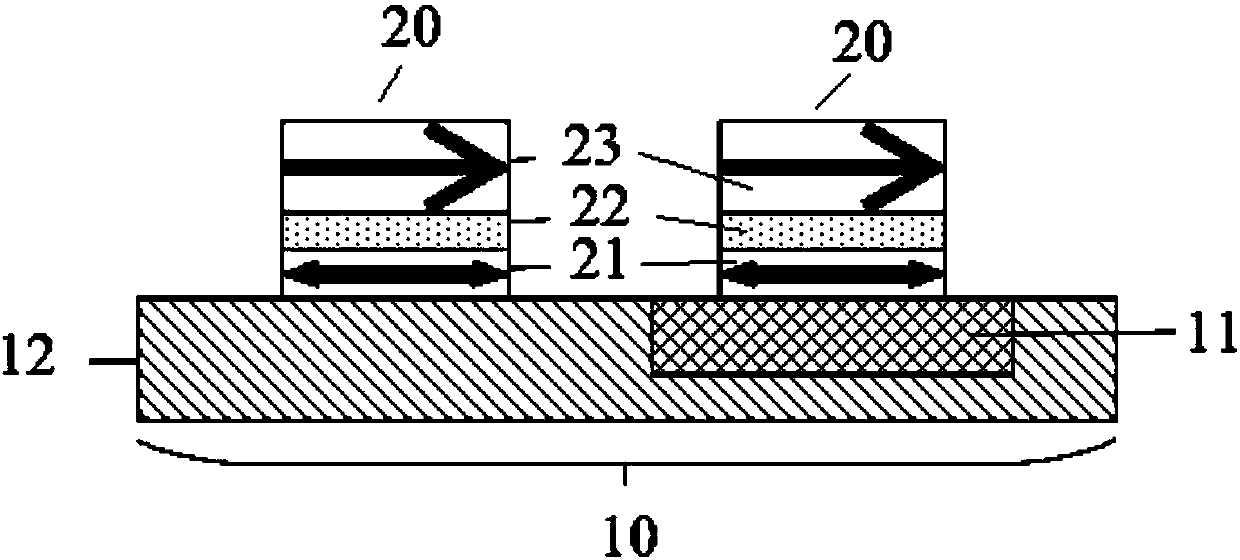
[0084] Such as Figure 9 As shown, the storage unit includes a spin-orbit moment providing structure 10 and two storage structures 20, which are respectively a first storage structure and a second storage structure. The spin-orbit moment providing structure 10 includes a first spin-orbit moment providing line 11 With the second spin-orbit moment supply line 12, the structures of the two storage structures 20 are the same, such as Figure 10 As shown, it includes a free layer 21, a tunnel layer 22, and a pinned layer 23 from bottom to top, wherein the free layer 21 of the first storage structure is arranged in contact with the first spin-orbit moment supply line 11, and the free layer of the second storage structure 21 is arranged in contact with the second spin-orbit moment supply line 12 . Such as Figure 10 As shown, the magnetization directions of the free layer 21 and the pinned layer 23 in each storage structure 20 are both perpendicular to the thickness of the storage ...
Embodiment 2
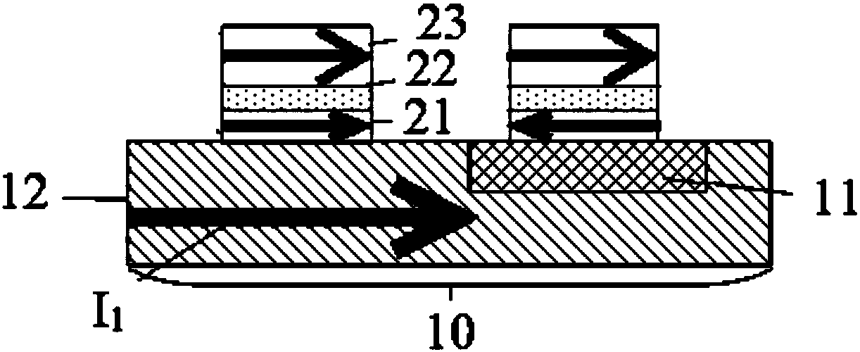
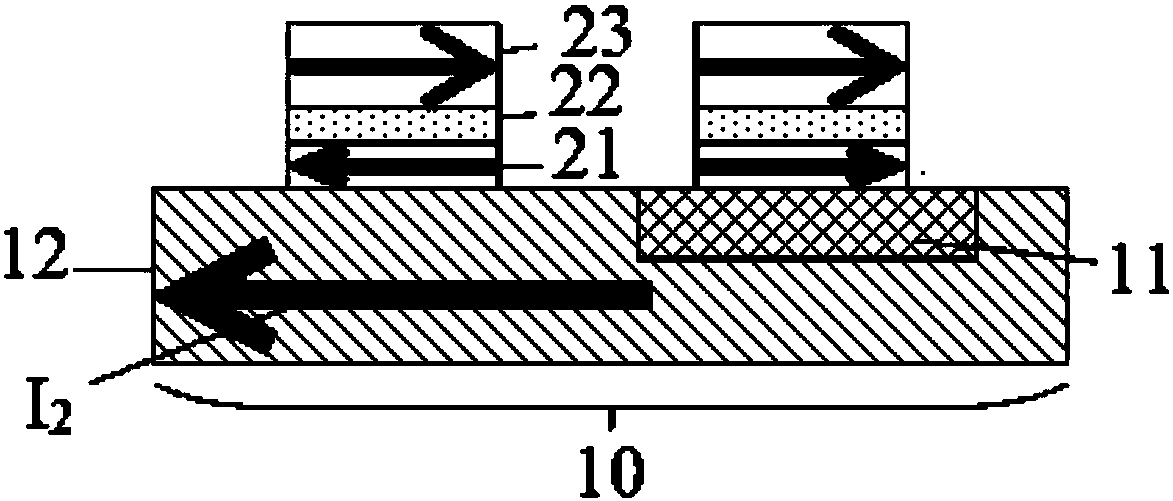
[0090] The spin-orbit moment providing structure 10 is the same as that in Embodiment 1, and the two storage structures 20 are respectively the first storage structure and the second storage structure. The structures of the two storage structures 20 are the same, as Figure 4 As shown, it includes a free layer 21, a tunnel layer 22, and a pinned layer 23 from bottom to top, wherein the free layer 21 of the first storage structure is arranged in contact with the first spin-orbit moment supply line 11, and the free layer of the second storage structure 21 is arranged in contact with the second spin-orbit moment supply line 12 . Such as Figure 4 As shown, the magnetization directions of the free layer 21 and the pinned layer 23 in each storage structure 20 are perpendicular to the thickness of the storage structure 20 , and are parallel or antiparallel to the write current direction of the spin-orbit moment providing structure 10 .
[0091] Each layer in each storage structure ...
Embodiment 3
[0095] The difference with embodiment 2 is that, as Figure 5 As shown, the storage structure further includes a magnetization layer 24 , and the magnetization layer is used to provide a magnetic field parallel to the thickness direction of the storage structure 20 .
[0096] The bias magnetic field provided by the magnetization layer causes the magnetization direction of the free layer to deviate from the plane of the memory cell, ie provides symmetry breaking. The torque of the free layer magnetic moment subjected to the equivalent field includes a horizontal component, which can ensure a one-to-one correspondence between the final magnetization direction of the free layer and the direction of the write current.
PUM
| Property | Measurement | Unit |
|---|---|---|
| Thickness | aaaaa | aaaaa |
| Thickness | aaaaa | aaaaa |
| Thickness | aaaaa | aaaaa |
Abstract
Description
Claims
Application Information