Method for flash technology high-voltage bar oxygen and tunnel-penetration oxidation layer

A technology of tunneling oxide layer and gate oxide layer, which is applied in the direction of electrical components, semiconductor/solid-state device manufacturing, circuits, etc., can solve the problems of reduced erasability, failure, and inability to erase, and achieve the goal of increasing the erasable number of times Effect

Active Publication Date: 2010-05-12
SHANGHAI HUAHONG GRACE SEMICON MFG CORP +1
View PDF7 Cites 0 Cited by
  • Summary
  • Abstract
  • Description
  • Claims
  • Application Information

AI Technical Summary

Problems solved by technology

As the number of erasing and writing increases, the charge traps in the tunnel oxide layer will increase accordingly, so that more and more electrons are trapped in the charge traps during the tunneling process, so that the electric field between the control gate and the floating gate The strength is reduced due to the shielding of the trapped charges, the erasability is continuously reduced, and eventually it fails because it cannot be erased

Method used


Image

  • Method for flash technology high-voltage bar oxygen and tunnel-penetration oxidation layer
  • Method for flash technology high-voltage bar oxygen and tunnel-penetration oxidation layer
  • Method for flash technology high-voltage bar oxygen and tunnel-penetration oxidation layer

Examples


Embodiment Construction

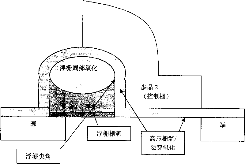
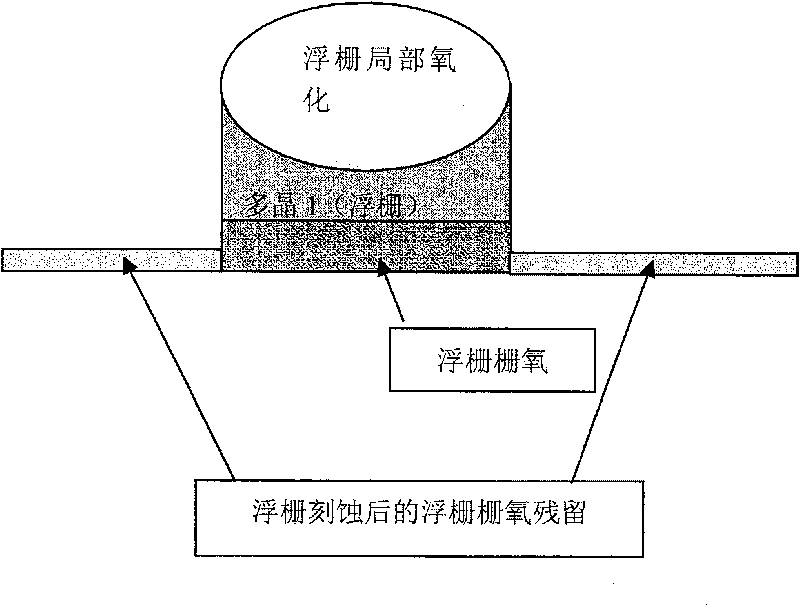
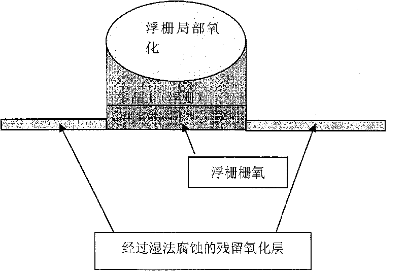
[0017] Reducing the thickness of the tunnel oxide layer, under the same working conditions, not only directly enhances the electric field strength during erasing, but also reduces the number of traps in the oxide layer, which is conducive to improving the erasing ability of the memory cell, thereby increasing its erasing and writing times . When the tunnel oxide thickness is reduced to , its erase and write times can reach 200,000 times.

[0018] However, the thickness of the high-voltage oxide layer must meet the withstand voltage requirements of the high-voltage transistor. Since flash memory uses a voltage as high as 12-14V, the total thickness of the high-voltage gate oxide layer needs to be greater than In order to ensure its normal operation and reliability requirements. In the current process in which the high-voltage gate oxide and the tunnel oxide layer are formed simultaneously, it is difficult to further reduce the thickness of the tunnel oxide layer.

[0019]...


PUM


Abstract

The invention discloses a flash memory technology high pressure gate oxide and tunneling oxide formation method, which comprise the steps of firstly retaining a floating boom gate oxide after floatingboom etching, with the thickness of 50-70 and eroding the floating boom gate oxide by the wet method and retaining the thickness of 20-30; then utilizing high temperature pressure reducing chemical vapor deposition method to form the tunneling oxide and the high pressure gate oxide simultaneously; at last forming the tunneling oxide with the thickness of 160-180 and the gate oxide with the high pressure of 180-210. The invention can improve electric field intensity in erasing, reduce oxide trap number and is good for the erasing capability improvement of storage unit, by reducing the thickness of the tunneling oxide.

Description

technical field [0001] The invention relates to a semiconductor integrated circuit process method, in particular to a method for forming a high-voltage gate oxide and a tunnel oxide layer in a flash memory process. Background technique [0002] As a main non-volatile memory, flash memory is widely used in smart cards, microcontrollers and other fields. Compared with EEPORM, another non-volatile memory, flash memory has obvious advantages in area; but at the same time, the reliability of flash memory, especially the erasable number of times, is worse than EEPROM, so it is used in bank cards, ID cards, etc. Product has not yet been used. [0003] SST flash memory is a type of flash memory invented by Bing Yeh in 1990 (US Patent No. 5029130), and the structure of its storage unit is as follows figure 1 shown. Among them, polycrystalline 1 is a floating gate, and the following is Thick floating gate oxide layer. A part of the polycrystalline 2 is covered on the floating ga...

Claims


Application Information

Patent Timeline
Patent Type & Authority Patents(China)
IPC IPC(8): H01L21/336H01L21/28H01L21/31H01L21/8247
Inventor 杨斌李铭龚新军杨鹏
Owner SHANGHAI HUAHONG GRACE SEMICON MFG CORP
Why Eureka
Try Eureka