Electron injection enhanced dual-mode MOS controlled thyristor and manufacturing method thereof

An electron injection and enhanced technology, applied in semiconductor/solid-state device manufacturing, circuits, electrical components, etc., can solve the problem that it is difficult to effectively reduce the on-state voltage drop of the device and improve the turn-off speed, and cannot meet the requirements of high-voltage and high-power switching applications, etc. problems, to achieve the effect of easy popularization and utilization, ingenious structural design, and low process cost

Active Publication Date: 2019-09-06
合肥森思功率半导体有限公司
View PDF6 Cites 1 Cited by
  • Summary
  • Abstract
  • Description
  • Claims
  • Application Information

AI Technical Summary

Problems solved by technology

[0004] The purpose of the present invention is to provide an electron injection enhanced dual-mode MOS control thyristor, which solves the problem that the device structure in the prior art is difficult to effectively reduce the on-state voltage drop of the device and increase the turn-off speed, and cannot meet the application requirements of high-voltage and high-power switches. The problem

Method used


Image

  • Electron injection enhanced dual-mode MOS controlled thyristor and manufacturing method thereof
  • Electron injection enhanced dual-mode MOS controlled thyristor and manufacturing method thereof
  • Electron injection enhanced dual-mode MOS controlled thyristor and manufacturing method thereof

Examples


Embodiment Construction

[0029] The present invention will be described in detail below in conjunction with the accompanying drawings and specific embodiments.

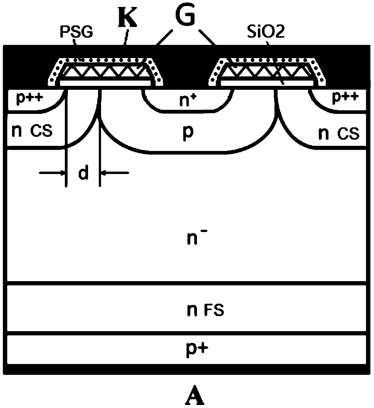
[0030] refer to figure 1 , the basic structure of the IE-Bi-MCT of the present invention is that the whole device is n - Drift region as substrate, n - A p base area is set in the center above the drift region, and an n base area is set in the center above the p base area. + Cathode area; the p base area is surrounded by an n CS layer (i.e., an n carrier storage layer), and the upper part of the n CS layer is provided with a p ++ shunt area, p ++ The aluminum layer on the upper surface of the shunt area is connected to the aluminum layer on the upper surface of the n+ cathode area to form the cathode electrode K; part n + Cathode region, p base region, n CS layer and part of p ++ A layer of gate oxide layer (i.e. SiO 2 Material layer), a heavily doped polysilicon layer is arranged on the upper surface of the gate oxide layer, and the po...


PUM


Abstract

The invention discloses an electron injection enhanced dual-mode MOS controlled thyristor. An n<+> cathode region is arranged inside a p base region in the center of the upper part of an n<-> drift region; a p<++> shunt region is arranged outside the upper part of an n CS layer around the periphery of the p base region, and a cathode electrode K is formed by aluminum layers on the upper surface ofthe p<++> shunt layer and the upper surface of the n<+> cathode region together; the upper surfaces of a part of the n<+> cathode region, the p base region, the n CS layer and a part of the p<++> shunt region are provided with a gate oxide layer together, and a polycrystalline silicon layer is arranged on the upper surface of the gate oxide layer as a grid electrode G; a phosphorosilicate glass layer is arranged between the cathode electrode K and the grid electrode G; and the n<-> drift region is provided with an n FS layer, a p<+> anode region and a metallized anode A downwards in sequence.The invention also discloses a preparation method of an IE-Bi-MCT. According to the IE-Bi-MCT structure disclosed by the invention, the on-state voltage drop of the device can be reduced obviously, and the cellular maximum controllable current is improved.

Description

technical field [0001] The invention belongs to the technical field of power semiconductor devices, and relates to an electron injection-enhanced dual-mode MOS control thyristor, and also relates to a manufacturing method of the electron injection-enhanced dual-mode MOS control thyristor. Background technique [0002] For high-voltage and high-power semiconductor devices, reducing their on-state voltage drop and conduction loss is very critical. Compared with the traditional thyristor, although the insulated gate bipolar transistor (IGBT) can increase the switching speed of the device, its on-state voltage drop is higher; although the MOS-controlled thyristor (MCT) can reduce its on-state voltage drop, the process Difficulty; base resistance controlled thyristor (BRT) can solve the difficult problem of MCT process, and its on-state voltage drop is also similar to MCT, but due to the wide cathode area of ​​BRT, the current distribution in it is uneven, and the device cannot b...

Claims


Application Information

Patent Timeline
Patent Type & Authority Applications(China)
IPC IPC(8): H01L29/745H01L29/749H01L21/332
CPCH01L29/7455H01L29/749H01L29/66363
Inventor 王彩琳杨武华曹荣荣
Owner 合肥森思功率半导体有限公司
Why Eureka
Try Eureka