A gate-controlled bipolar-field-effect compound element semiconductor-based lateral double-diffused metal oxide semiconductor transistor
A lateral double diffusion, semiconductor technology, applied in the direction of semiconductor devices, electrical components, circuits, etc., to achieve the effect of increasing on-current, reducing on-resistance, and preventing secondary breakdown
- Summary
- Abstract
- Description
- Claims
- Application Information
AI Technical Summary
Problems solved by technology
Method used
Image
Examples
Embodiment Construction
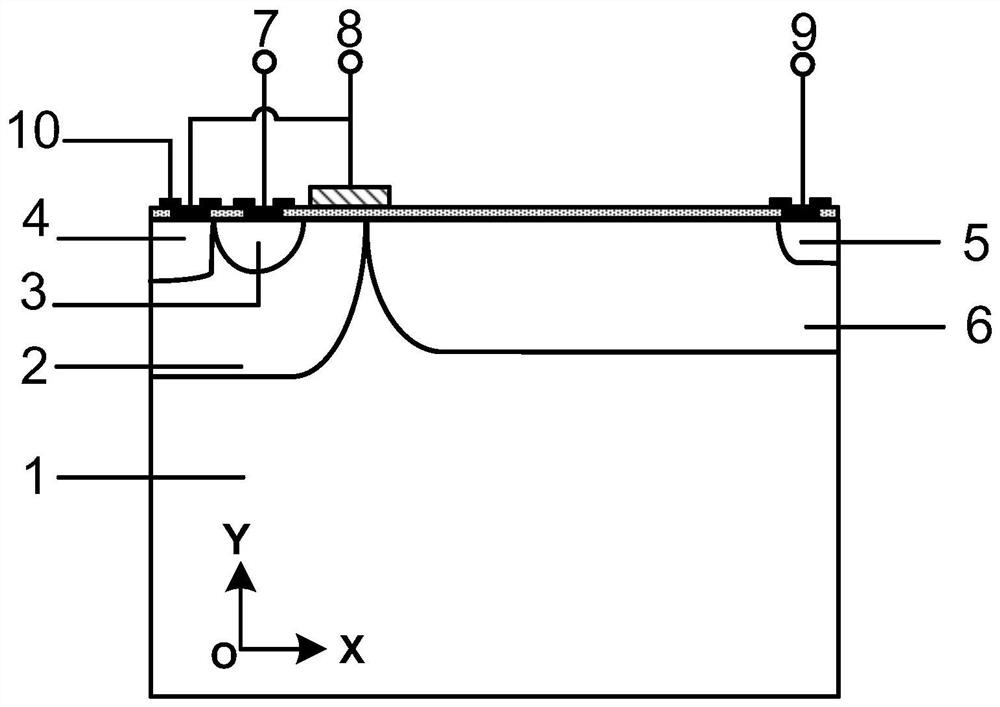
[0029] like figure 1 As shown, the gate-controlled bipolar-field-effect compound element semiconductor-based lateral double-diffused metal-oxide-semiconductor transistor:
[0030] Elemental semiconductor substrate 1, specifically silicon or germanium, with a doping concentration of 1×10 13 cm -3 ~1×10 15 cm -3 ;
[0031] An epitaxial layer is formed on the substrate 1; the specific material is silicon or germanium, and the doping concentration is 1×10 15 cm -3 ~1×10 16 cm -3 ;
[0032] forming a base region 2 on the epitaxial layer;
[0033] Forming an active region on the surface of the device;
[0034] a gate insulating layer formed on the active region, and forming a gate 8 above the gate insulating layer;
[0035] A source region 3 and a base region contact 4 are formed on the base region while a channel is formed on the base region; wherein, the doping concentration of the base region contact is 1×10 20 cm -3 ;
[0036] forming a drain region 5 on the drift ...
PUM
 Abstract
Description
Claims
Application Information

