Double-swing-arm die-bonding device for LED die bonding and die bonding method thereof

A double-swing arm and LED bracket technology, which is applied to electrical components, circuits, semiconductor devices, etc., can solve the problems of reduced speed and precision, increased inertia, and low work efficiency, and achieves good adaptability, compact structure, and improved solid state. Effect of Crystal Efficiency

Pending Publication Date: 2019-09-10
SHENZHEN XINYICHANG AUTOMATIC EQUIP
View PDF0 Cites 8 Cited by
  • Summary
  • Abstract
  • Description
  • Claims
  • Application Information

AI Technical Summary

Problems solved by technology

In this way of working, since only one LED chip can be picked up and transported at a time, the working efficiency is low and the speed of solid crystal is slow.
And for the die bonding of large-sized LED brackets, the traditional die-bonding method often needs to increase the length and weight of the swing arm to meet the die-bonding requirements. Decrease in speed and accuracy

Method used


Image

  • Double-swing-arm die-bonding device for LED die bonding and die bonding method thereof
  • Double-swing-arm die-bonding device for LED die bonding and die bonding method thereof
  • Double-swing-arm die-bonding device for LED die bonding and die bonding method thereof

Examples


Embodiment 1

[0049] Example 1. The specific structure of the present invention is as follows:

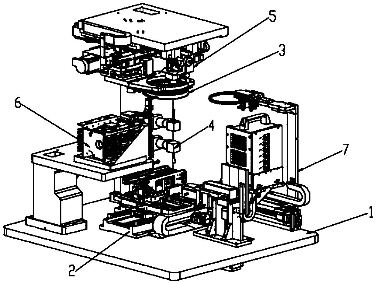
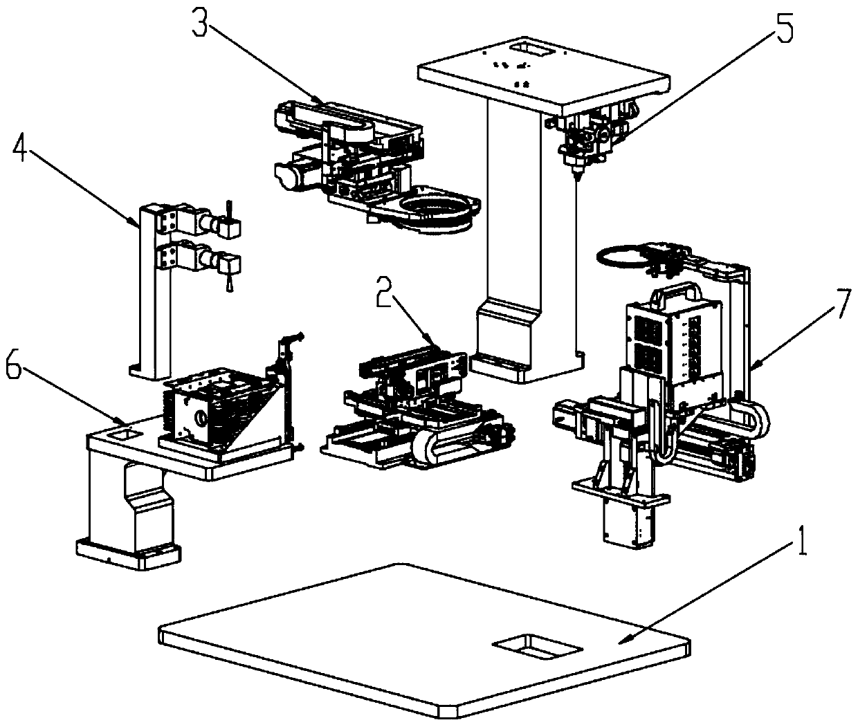
[0050] Please refer to the attached Figure 1-8 , A double-swing arm die-bonding device for LED die bonding of the present invention, the double-swing arm die-bonding device includes:

[0051] Platen 1;

[0052] It also includes those set on the platen 1:

[0053] The die-bonding mechanism 6 is provided with two die-bonding pendulum arms 6-4, a telescopic drive mechanism 6-3 that drives the two die-bonding pendulum arms 6-4 to move toward or in the opposite direction, and connects and drives the telescopic drive mechanism 6-3 The rotation driving mechanism 6-2 that drives the two die-bonding swing arms 6-4 to rotate;

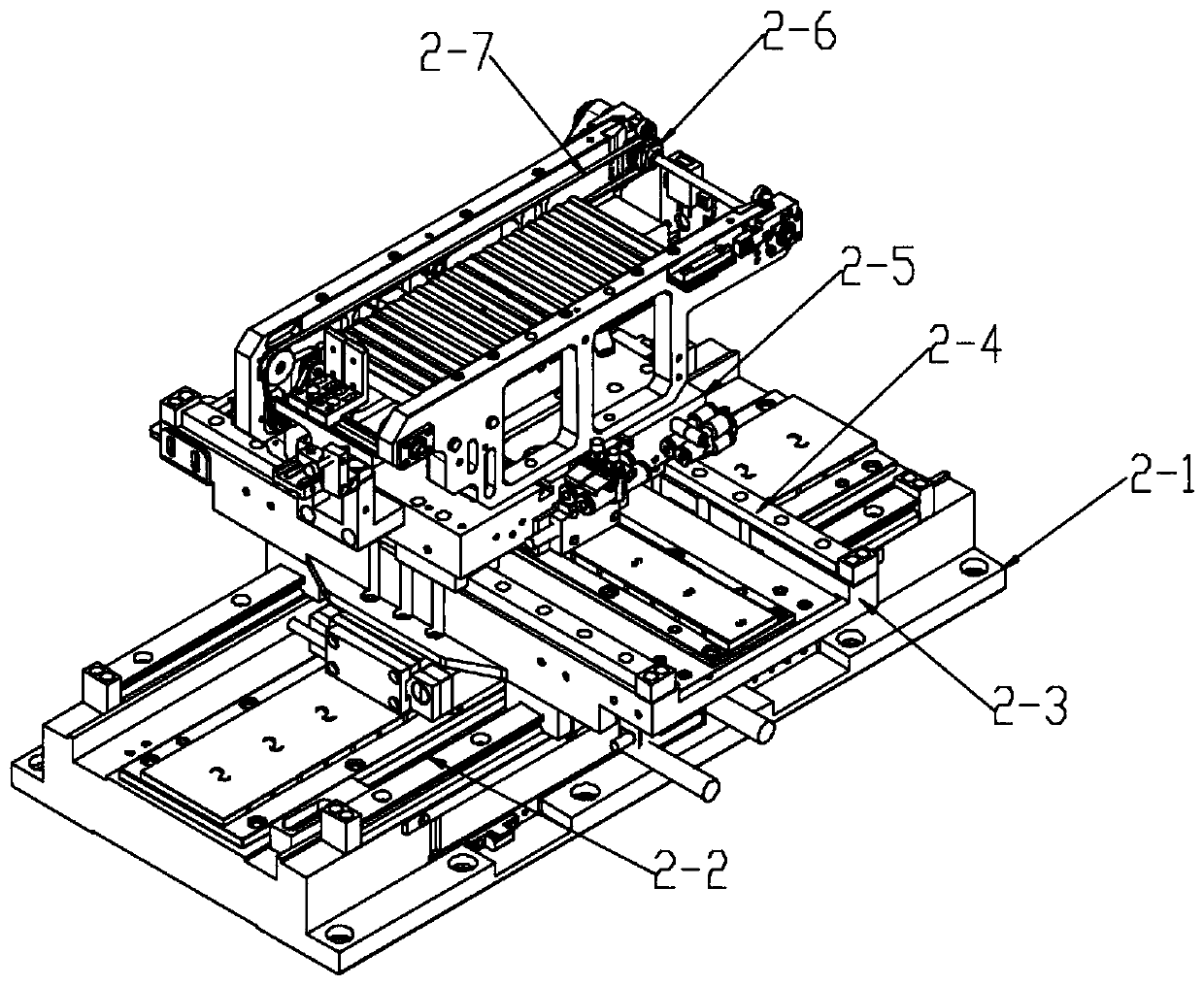
[0054] The fixture moving platform 2 is arranged on the adjacent side of the crystal bonding mechanism 6, and is provided with a first transverse slide rail mechanism, a first longitudinal slide rail mechanism seated on the first transverse slide rail mechanism, and a The pulley assembly...

Embodiment 2

[0072] Embodiment 2: A method for bonding a dual-swing arm bonding device of an LED bonding machine of the present invention, the method includes the following steps:

[0073] Step 1: With the assistance of the die-bonding lens assembly 4-2, the system controls the fixture moving platform 2 to move horizontally and vertically to drive the LED bracket on it to move to the die-attach position;

[0074] Step 2: With the assistance of the crystal lens assembly 4-1, the system control ring mobile platform assembly 3 performs horizontal and vertical movement, thereby driving the crystal ring located on it to move to the specified position and correct it;

[0075] Step 4: The rotary drive mechanism 6-2 drives one of the die-bonding swing arms 6-4 to rotate and move to the top of the wafer, the ejector pin assembly 5 ejects an LED chip on the die ring, and the driven die-bonding swing arm 6 -4 Take the ejected chip and rotate it 180° to fix it on the LED bracket. At the same time, another di...


PUM


Abstract

The invention discloses a double-swing-arm die-bonding device for LED die bonding and a die bonding method thereof. The die-bonding device comprises a table board, and a double-swing-arm die-bonding mechanism arranged on the table board, wherein a crystal ring moving platform is arranged above the double-swing-arm die-bonding mechanism, and a clamp moving platform is arranged below the double-swing-arm die-bonding mechanism; an automatic crystal ring feeding mechanism is arranged on one side of the clamp moving platform, while a lens assembly is arranged on the other side of the clamp moving platform; and an ejector pin assembly is further arranged above the crystal ring moving platform. The lens assembly is used for assisting the crystal ring moving platform and a clamp to move to a designated position. The ejector pin assembly is used for ejecting an LED wafer on the crystal ring moving platform; the double-swing-arm die-bonding mechanism drives the two die-bonding arms to rotate ina plane perpendicular to the horizontal plane, and then sucks ejected wafers to fix the ejected wafers to an LED bracket; the automatic crystal ring feeding mechanism is used for feeding or recoveringthe crystal ring; and compared with a traditional crystal fixing mode, the die bonding device is used for carrying out continuous die bonding by arranging the two die-bonding swing arms to rotate, sothat the die bonding speed is increased, and the application range is wide.

Description

Technical field [0001] The invention relates to LED processing equipment, in particular to a double-swing arm die-bonding device for LED die-bonding and a die-bonding method thereof. Background technique [0002] Light Emitting Diode (LED) is a light emitting element that can convert electrical energy into light energy. LED products can be used in many fields such as lighting, display, and signal indication. With the continuous development of LED technology, the requirements for LED die-bonding speed are getting higher and higher. [0003] The current LED chip bonding process is as follows: Since the LED chips are usually glued to the crystal ring film by the supplier, first the ejector pin mechanism lifts the designated LED chip from the crystal ring film, and then the chip is fixed by the chip bonding mechanism. The crystal swing arm rotates horizontally to directly above the designated LED chip, and then moves up and down to absorb the designated LED chip on the crystal ring f...

Claims


Application Information

Patent Timeline
IPC IPC(8): H01L33/48
CPCH01L33/48H01L2933/0033
Inventor 胡新荣梁志宏胡新平陈玮麟
Owner SHENZHEN XINYICHANG AUTOMATIC EQUIP
Why Eureka
Try Eureka