Display panel, crystal coating thin film and display device

A display panel and chip-on-film technology, which is used in identification devices, instruments, nonlinear optics, etc., can solve the problems of waste of space and large height of the lower frame of the display substrate, and achieve the effect of improving space utilization.

Active Publication Date: 2019-09-10
BOE TECH GRP CO LTD +1
View PDF5 Cites 10 Cited by
  • Summary
  • Abstract
  • Description
  • Claims
  • Application Information

AI Technical Summary

Problems solved by technology

[0003] However, in the existing COF binding method, the height of the fanout lead area connecting the COF binding area and the effective display area is relatively large, resulting in a waste of space on the lower border of the display substrate.

Method used


Image

  • Display panel, crystal coating thin film and display device
  • Display panel, crystal coating thin film and display device
  • Display panel, crystal coating thin film and display device

Examples


Embodiment Construction

[0039] In order to make the above objects, features and advantages of the present invention more comprehensible, the present invention will be further described in detail below in conjunction with the accompanying drawings and specific embodiments.

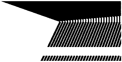
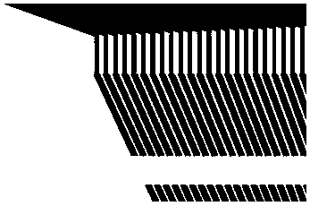
[0040] The inventors have found that the cause of the large height of the fanout lead region in the related art is related to the pin structure of the bonding region. Such as figure 2 As shown, in order to compensate for the thermal deformation of the flexible substrate, the COF pin in the flexible OLED product COF bonding method is designed to be inclined, and the overall shape is a trapezoidal structure with the short side close to the effective display area. Such as image 3 As shown, in this structure, the connection position between the outermost COF Pin and the fanout trace (that is, the outermost trace outlet point a) is close to the middle of the COF, and if the Y-direction compensation of the process is considered, the ...


PUM


Abstract

The invention provides a display panel, a crystal coating thin film and a display device. The display panel comprises an effective display area and a binding area; the display panel of the binding area comprises a first substrate and at least one row of first pins arranged on one side of the first substrate, wherein the distance of one ends, close to the effective display area, of the two adjacentfirst pins in the same row is larger than the distance of one ends, away from the effective display area; the whole body is of an inverted trapezoid structure with the long edge being close to the effective display area, so that the outermost lead of a fanout area is close to the edge of the display panel; compared with a regular trapezoid structure, with the short side being close to the effective display area, of the pin of the existing binding area, the vertical wire of the fanout area lead is longer, and a lower frame can be realized by shortening the height of the vertical wire; or underthe condition of the same frame, more design spaces can be reserved for other circuit units by shortening the vertical wire height, so that the space utilization rate of the display substrate can beimproved.

Description

technical field [0001] The invention relates to the field of display technology, in particular to a display panel, a chip-on-chip film and a display device. Background technique [0002] As flexible display products become more and more popular, flexible display products are developing towards higher resolution and ultra-narrow bezels. In order to realize the narrowing of the driving side frame of the flexible display device, in the current manufacturing process, the driving chip is generally bonded in two ways, namely COF (Chip On Film, such as figure 1 shown) and COP (Chip On Plastic). Compared with the COP bonding method, the pins in the COF bonding method have a smaller bonding pitch, and there is no need to bind the pins on the backplane design to ILB, flexible board FPC and other areas, which can save display on the backplane The lower frame of the device is beneficial to increase the number of layouts and improve the utilization rate of the backplane glass. In addi...

Claims


Application Information

Patent Timeline
Patent Type & Authority Applications(China)
IPC IPC(8): H01L51/52H01L27/32G09F9/30
CPCG09F9/301H10K59/00H10K59/131H10K50/84H10K50/844G06F1/1652G06F1/189G02F1/13452H05K1/111
Inventor 周宏军
Owner BOE TECH GRP CO LTD
Why Eureka
Try Eureka