PCB centre template automatic design method and system, storage medium and terminal

A PCB board, automatic design technology, applied in CAD circuit design, computer-aided design, calculation and other directions, can solve the problems of high experience requirements, inaccuracy, time-consuming placement, etc., to reduce the probability of errors, reduce labor costs, and apply wide range of effects

Active Publication Date: 2019-09-17
VAYO SHANGHAI TECH
View PDF6 Cites 1 Cited by
  • Summary
  • Abstract
  • Description
  • Claims
  • Application Information

AI Technical Summary

Problems solved by technology

[0007](1) The position of the thimble is judged entirely by manual or measuring tools, which takes a long time and is inaccurate. For example, for components with a height greater than amm, The thimble placement distance must be greater than bmm. Designers need to screen out devices with a height greater than amm according to the PCB design drawings, and then use measuring tools to determine the prohibited range and then arrange thimbles;
[0008](2) The experience requirements for designers are relatively high, and the thimble templates designed are thousands of people, so standardized design cannot be realized;
[0009](3) Extended product development cycle and reduced product quality

Method used


Image

  • PCB centre template automatic design method and system, storage medium and terminal
  • PCB centre template automatic design method and system, storage medium and terminal
  • PCB centre template automatic design method and system, storage medium and terminal

Examples


Embodiment Construction

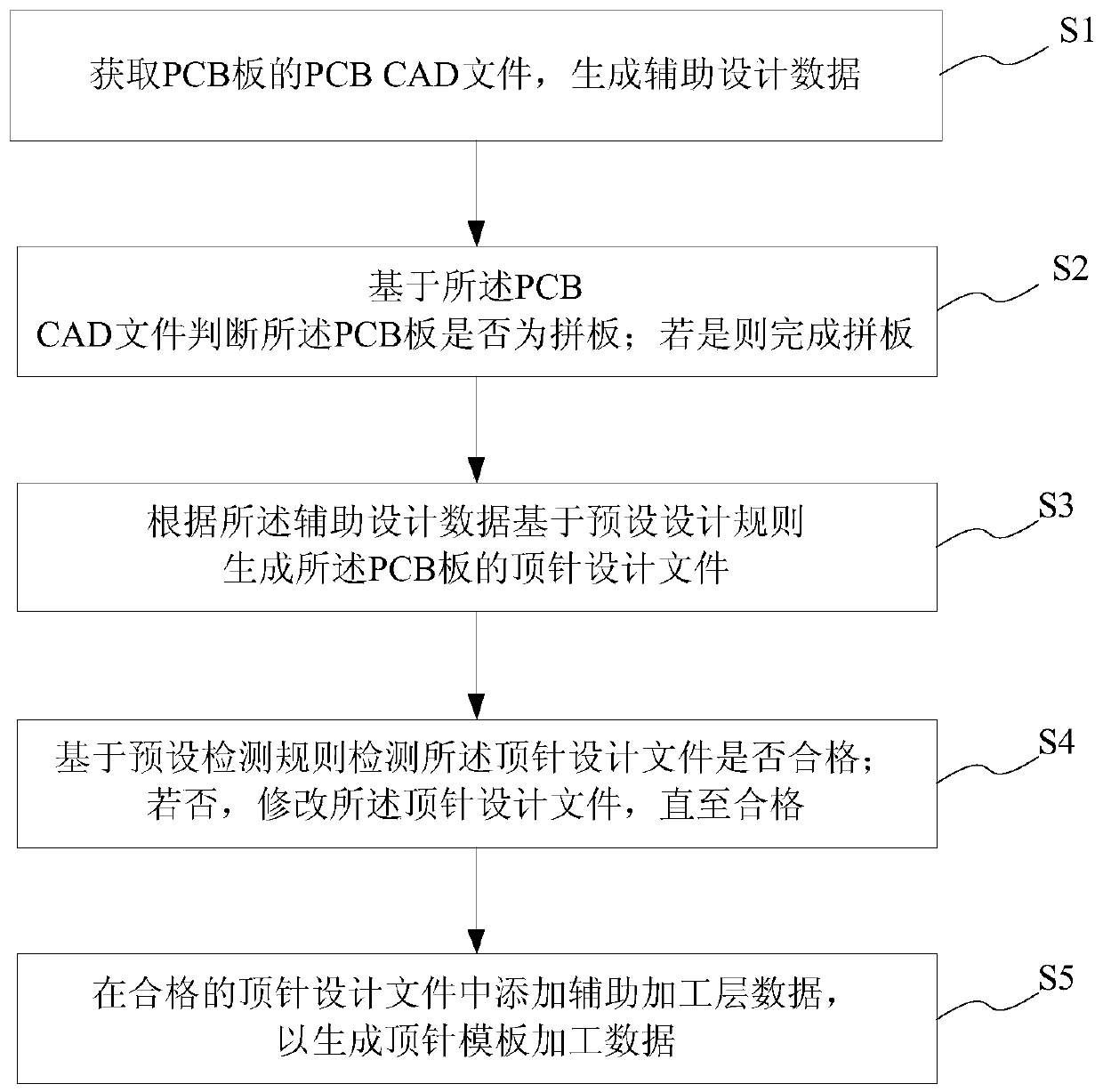
[0058] Embodiments of the present invention are described below through specific examples, and those skilled in the art can easily understand other advantages and effects of the present invention from the content disclosed in this specification. The present invention can also be implemented or applied through other different specific implementation modes, and various modifications or changes can be made to the details in this specification based on different viewpoints and applications without departing from the spirit of the present invention. It should be noted that, in the case of no conflict, the following embodiments and features in the embodiments can be combined with each other.

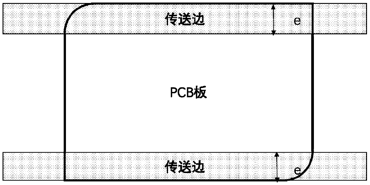
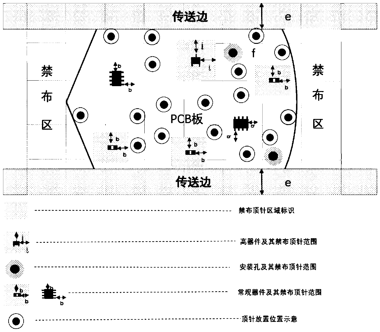
[0059] It should be noted that the diagrams provided in the following embodiments are only schematically illustrating the basic ideas of the present invention, and only the components related to the present invention are shown in the diagrams rather than the number, shape and shape of the compo...


PUM


Abstract

The invention provides a PCB centre template automatic design method and system, a storage medium and a terminal, and the method comprises the following steps: obtaining a PCB CAD file of a PCB, and generating auxiliary design data; judging whether the PCB is a jointed board or not based on the PCB CAD file; if yes, completing board splicing; generating a centre design file of the PCB based on a preset design rule according to the auxiliary design data; detecting whether the centre design file is qualified or not based on a preset detection rule; if not, modifying the centre design file until the centre design file is qualified; and adding auxiliary processing layer data into the qualified centre design file to generate centre template processing data. According to the PCB centre template automatic design method and system, the storage medium and the terminal, manual intervention is not needed, automatic PCB centre template design can be achieved, and practicability is high.

Description

technical field [0001] The present invention relates to the technical field of printed circuit boards (Printed Circuit Board, PCB), in particular to an automatic design method and system for a PCB thimble template, a storage medium and a terminal. Background technique [0002] Surface Mounting Technology (SMT) is a method of mounting surface mount components packaged in a matrix arrangement without leads or short leads or balls on the surface of a PCB or on the surface of other substrates, through reflow soldering or dip soldering, etc. The method is a circuit assembly technology of soldering assembly. Among them, in the process of automatic solder paste printing and placement, it is necessary to support the unprocessed surface of the PCB board with thimbles before processing. With the change of market demand and the development of science and technology, electronic products will become smaller and shorter, and the product cycle will be shorter and shorter. Not only the PCB...

Claims


Application Information

Patent Timeline
Patent Type & Authority Applications(China)
IPC IPC(8): G06F17/50
CPCG06F30/398G06F30/39
Inventor 刘继硕刘久轩宋勇强刘丰收
Owner VAYO SHANGHAI TECH
Why Eureka
Try Eureka