Semiconductor structure and formation method thereof

A semiconductor and channel structure technology, which is applied in semiconductor devices, semiconductor/solid-state device manufacturing, semiconductor/solid-state device components, etc., can solve problems such as device performance degradation, improve performance, improve heat dissipation performance, and improve self-heating effect Effect

Active Publication Date: 2019-09-24
SEMICON MFG INT (SHANGHAI) CORP +1
View PDF3 Cites 7 Cited by
  • Summary
  • Abstract
  • Description
  • Claims
  • Application Information

AI Technical Summary

Problems solved by technology

[0005] However, after the introduction of SiGe channel techno

Method used


Image

  • Semiconductor structure and formation method thereof
  • Semiconductor structure and formation method thereof
  • Semiconductor structure and formation method thereof

Examples


Embodiment Construction

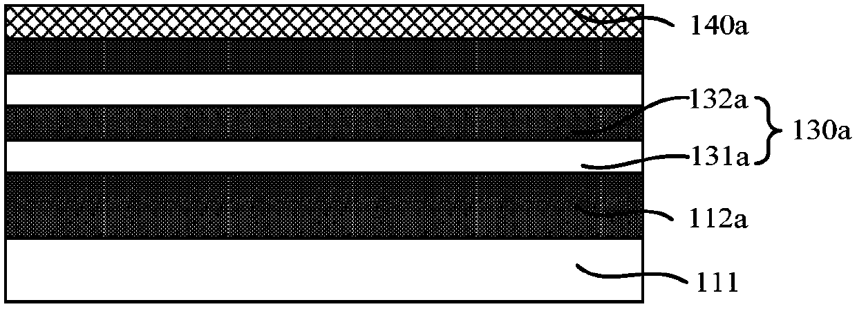
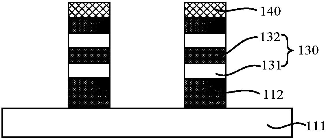
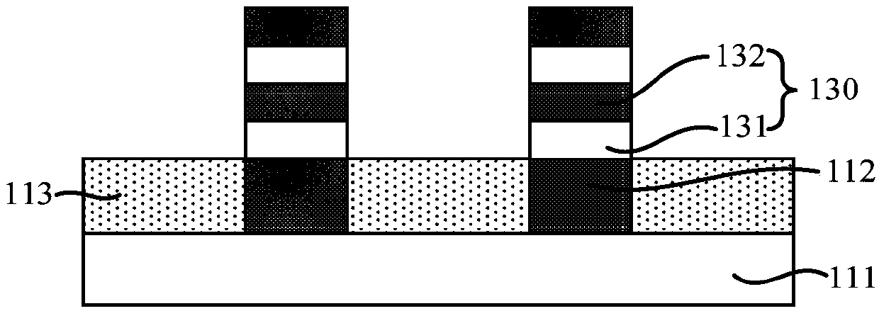
[0014] It can be seen from the background art that the introduction of the SiGe channel technology will easily lead to the degradation of device performance. Analyze the reasons for this:

[0015] Compared with Si, SiGe has a lower thermal conductivity. Therefore, after the introduction of SiGe channel technology, it is easy to cause the heat generated by the device to dissipate too late, thereby reducing the heat dissipation effect of the device.

[0016] Moreover, after the fin structure is introduced into the fully-enclosed gate transistor, compared with the planar transistor, the area occupied by the substrate of the fully-enclosed gate transistor is reduced, the area occupied by the isolation structure is increased, and the area occupied by the substrate is reduced. Small will reduce the heat dissipation effect of the device, and because the material of the isolation structure is usually silicon oxide, the thermal conductivity of silicon oxide is also low, which further d...


PUM

PropertyMeasurementUnit
Depthaaaaaaaaaa
Thicknessaaaaaaaaaa

Abstract

The invention relates to a semiconductor structure and a formation method thereof. The method comprises the steps of providing a base, wherein the base includes a substrate, discrete fins protruding out of the substrate and channel laminations on the fins, wherein each channel lamination include a sacrificial layer and a channel layer located on the sacrificial layer, the number of the channel laminations is one or more, and the fins and the channel layers are made from SiGe; forming a pseudo gate layer which crosses the channel laminations and covers the top and part of the side walls of the channel laminations; sequentially etching the channel laminations and the fin at two sides of the pseudo gate layer, forming a top groove inside the channel laminations, and forming a bottom groove, which exposes the substrate and is communicated with the top groove, inside the fin; forming a semiconductor layer in the bottom groove, wherein the heat conductivity coefficient of the semiconductor layer is greater than that of SiGe; and forming a doped epitaxial layer in the top groove after forming the semiconductor layer. The semiconductor layer with a higher heat conductivity coefficient is adopted to replace the SiGe fin at both sides of the pseudo gate layer, thereby improving the spontaneous heating effect, and thus improving the performance of PMOS (P-channel Metal Oxide Semiconductor) transistors.

Description

technical field [0001] The invention relates to the field of semiconductor manufacturing, in particular to a semiconductor structure and a forming method thereof. Background technique [0002] In semiconductor manufacturing, with the development trend of VLSI, the feature size of integrated circuits continues to decrease. In order to adapt to the reduction of feature size, the channel length of MOSFET (Metal-Oxide-Semiconductor Field-Effect Transistor, MOSFET) is also shortened correspondingly. However, as the channel length of the device is shortened, the distance between the source and the drain of the device is also shortened, so the control ability of the gate to the channel becomes worse, and the gate voltage pinches off the channel. The difficulty is also increasing, making the phenomenon of subthreshold leakage (subthreshold leakage), the so-called short-channel effect (SCE: short-channel effects) more likely to occur. [0003] Therefore, in order to better meet the...

Claims


Application Information

Patent Timeline
IPC IPC(8): H01L21/336H01L29/78H01L23/373
CPCH01L29/66795H01L29/785H01L23/3738
Inventor 周飞
Owner SEMICON MFG INT (SHANGHAI) CORP
Why Eureka
Try Eureka