AMOLED (Active-Matrix Organic Light Emitting Diode) display panel and preparation method thereof

A display panel and plasma technology, applied in semiconductor/solid-state device manufacturing, electrical components, electric solid-state devices, etc., can solve the problems of organic light-emitting layer 2 damage, organic light-emitting layer luminous efficiency reduction, failure, etc., to achieve enhanced water blocking effect , prolong the luminous efficiency and service life, and reduce the effect of damage

Inactive Publication Date: 2019-09-24
EVERDISPLAY OPTRONICS (SHANGHAI) CO LTD
View PDF5 Cites 0 Cited by
  • Summary
  • Abstract
  • Description
  • Claims
  • Application Information

AI Technical Summary

Problems solved by technology

At present, the structure of the traditional flexible organic light-emitting layer is a sandwich-type sandwich structure formed by "anode layer 1 / organic light-emitting layer 2 / cathode layer 3 / covering layer 4 / encapsulation layer TFE5" (such as figure 1 shown), wherein the organic light-emitting layer 2, the cathode layer 3 and the covering layer 4 are mainly prepared by evaporation, and TFE5 is a laminated structure in which the inorganic film layer 51 and the organic film layer 52 are stacked alternately, mainly through plasma It is prepared by Plasma Enhanced Chemical Vapor Deposition (PECVD for short) equipment, and the ions in the PECVD process will cause damage to the organic light-emitting layer 2, resulting in a decrease in the luminous efficiency of the organic light-emitting layer or even failure.

Method used


Image

  • AMOLED (Active-Matrix Organic Light Emitting Diode) display panel and preparation method thereof
  • AMOLED (Active-Matrix Organic Light Emitting Diode) display panel and preparation method thereof
  • AMOLED (Active-Matrix Organic Light Emitting Diode) display panel and preparation method thereof

Examples


Embodiment Construction

[0030] The technical solutions in the embodiments of the present invention will be clearly and completely described below with reference to the accompanying drawings in the embodiments of the present invention. Obviously, the described embodiments are only a part of the embodiments of the present invention, but not all of the embodiments. Based on the embodiments of the present invention, all other embodiments obtained by those of ordinary skill in the art without creative efforts shall fall within the protection scope of the present invention.

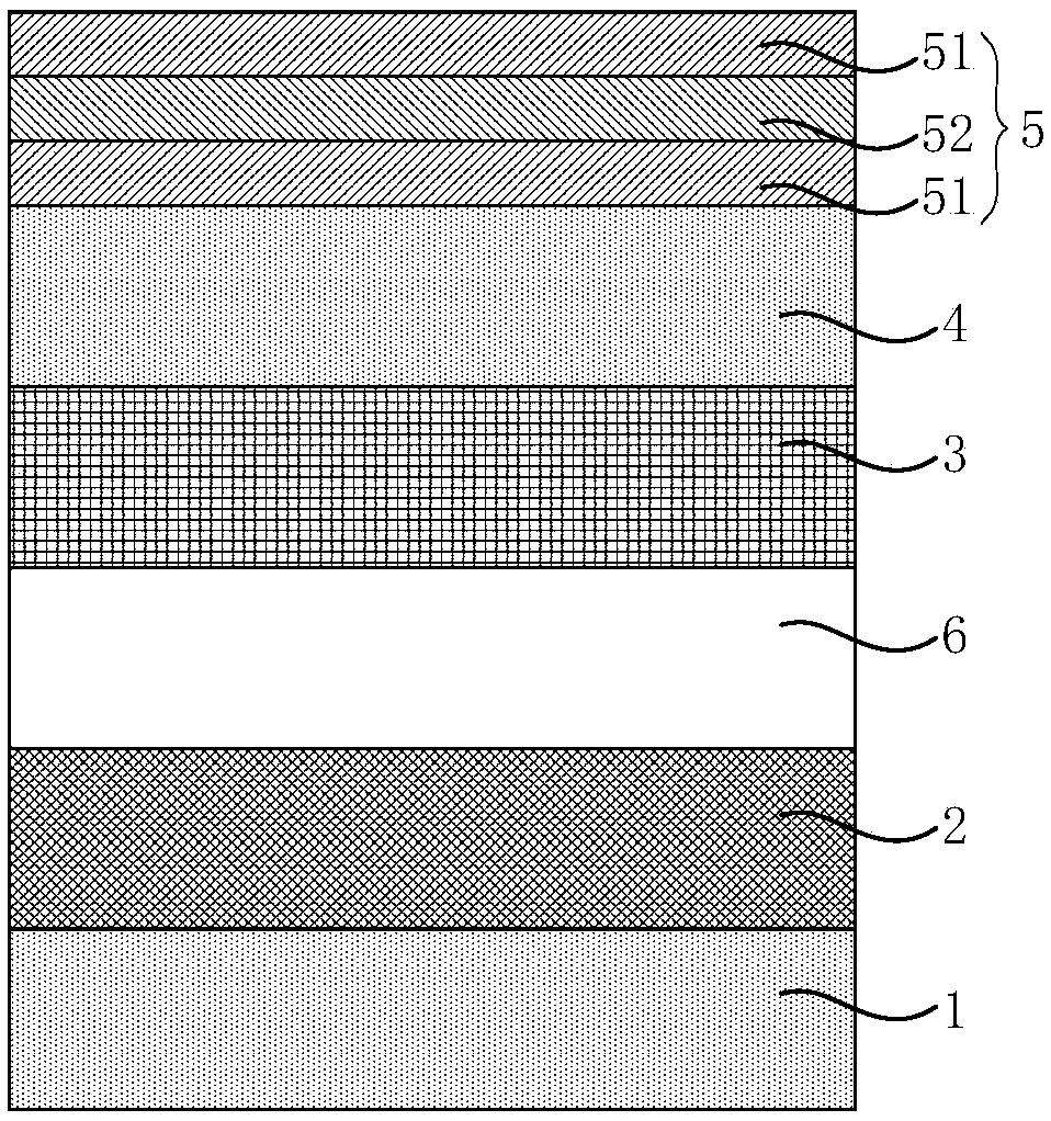
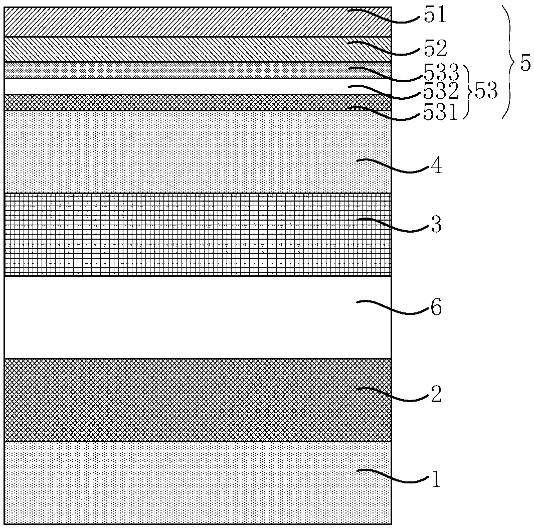
[0031] Please refer to figure 2 , the present invention provides an AMOLED display panel, which is formed with an anode layer 1, an organic light-emitting layer 2, a cathode layer 3, a cover layer 4 and an encapsulation layer TFE5 along the direction from the bottom layer to the top layer. The layer 51 is stacked in the direction from the bottom layer to the top layer to form a stack structure, and the layer of the stack structure in...


PUM


Abstract

The invention relates to the technical field of display, and discloses an AMOLED (Active-Matrix Organic Light Emitting Diode) display panel and a preparation method thereof. The display panel comprises an anode layer, an organic light emitting layer, a cathode layer, a covering layer and packaging layer TFE which are formed in the direction from the bottom layer to the top layer, the TFE includes at least one stack structure formed by stacking an organic film layer and an inorganic film layer in the direction from the bottom layer to the top layer, the film layer contacted with the covering layer of the stack structure is a first inorganic film layer, the first inorganic film layer includes three sub-film layers such as a plasma barrier layer, a coating layer and a water blocking layer, and the three sub-film layers such as the plasma barrier layer, the coating layer and the water blocking layer are sequentially arranged in the direction from the bottom layer to the top layer. Therefore, the display panel not only can enhance the water blocking effect, but also can avoid the damage to the organic light emitting layer during the TFE preparation process through optimizing the TFE structure, thereby being conducive to prolonging the service life of the organic light emitting layer, and improving the light emitting efficiency of the AMOLED display panel.

Description

technical field [0001] The present invention relates to the field of display technology, in particular to an AMOLED display panel and a preparation method thereof. Background technique [0002] In recent years, flat panel display technology has developed rapidly, and consumers' demands for color and lightness of display devices are also increasing. Active-matrix organic light emitting diode (AMOLED) displays have the advantages of flexibility, low energy consumption, ultra-thin and healthy eye protection, etc., and have become the development trend of next-generation display technology. As far as the industry is concerned, in the field of AMOLED, thin film packaging technology is one of its core technologies. [0003] Since AMOLEDs are very sensitive to water vapor and oxygen, the water vapor and oxygen permeating into the interior of the device are the main factors affecting the lifetime of AMOLEDs. Therefore, effective thin-film encapsulation of the organic light-emittin...

Claims


Application Information

Patent Timeline
Patent Type & Authority Applications(China)
IPC IPC(8): H01L27/32H01L51/52H01L51/56
CPCH10K59/12H10K50/844H10K71/00
Inventor 洪飞叶雪妮闫春花
Owner EVERDISPLAY OPTRONICS (SHANGHAI) CO LTD
Why Eureka
Try Eureka