Near-sensor visual perception processing chip and Internet of Things sensing device

A visual perception and processing chip technology, applied in the field of image processing, can solve the problems of high power consumption, low energy efficiency, and reduced performance of the perception system in processing solutions, so as to avoid the overhead of analog-to-digital conversion and improve energy efficiency.

Active Publication Date: 2019-09-27
TSINGHUA UNIV
View PDF9 Cites 9 Cited by
  • Summary
  • Abstract
  • Description
  • Claims
  • Application Information

AI Technical Summary

Problems solved by technology

However, due to the limitation of battery resources, especially when dealing with computationally intensive tasks applying artificial intelligence algorithms, it is often impossible for various AIoT devices to strike a balance between processing quality, real-time performance, power or energy constraints
[0003] In order to solve the above existing problems and improve the processing efficiency of AIoT devices in the field of edge computing, at present, the following methods are mainly used to realize the acquisition and processing of image data by AIoT device terminals: First, by using embedded computer graphics processing processor (GPU) or based on field-progr

Method used


Image

  • Near-sensor visual perception processing chip and Internet of Things sensing device
  • Near-sensor visual perception processing chip and Internet of Things sensing device
  • Near-sensor visual perception processing chip and Internet of Things sensing device

Examples


Embodiment Construction

[0021] In order to make the purposes, technical solutions and advantages of the embodiments of the present invention clearer, the technical solutions in the embodiments of the present invention will be clearly and completely described below with reference to the accompanying drawings in the embodiments of the present invention. Obviously, the described embodiments These are some embodiments of the present invention, but not all embodiments. Based on the embodiments of the present invention, all other embodiments obtained by those of ordinary skill in the art without creative efforts shall fall within the protection scope of the present invention.

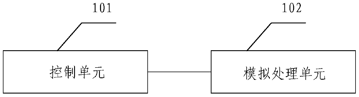
[0022] like figure 1 As shown, the embodiment of the present invention provides a proximity sensor visual perception processing chip, which includes but is not limited to: a control unit 101 and an analog processing unit 102; wherein the control unit 101 is used to input binarized analog data to the analog processing Unit 102, wher...


PUM


Abstract

The embodiment of the invention provides a near-sensor visual perception processing chip and an Internet of Things sensing device, wherein the chip comprises a control unit and an analog processing unit, the control unit is used for inputting the binarized analog data into the analog processing unit, the binarized analog data is composed of an analog voltage signal acquired by a sensor and a weight signal corresponding to the analog voltage signal, and the analog processing unit is used for processing the received binary analog data to obtain a current value corresponding to the analog voltage signal. The sensing device comprises a CMOS image sensor, the chip and a communication module. According to the near-sensor visual perception processing chip and the Internet of Things sensing device provided by the embodiment of the present invention, the analog processing unit adopting a binary neural network algorithm is placed behind the CMOS image sensor and in front of the ADC, so that the chip can directly process the analog voltage signals, the huge energy consumption during the analog-to-digital conversion is avoided, and the energy efficiency is effectively improved.

Description

technical field [0001] The invention relates to the technical field of image processing, in particular to a proximity sensor visual perception processing chip and an Internet of Things sensing device. Background technique [0002] With the rapid development of artificial intelligence, the current Intelligent Internet of Things (abbreviation: AIoT) has been widely used in our production and life. However, AIoT devices not only perceive image data at the terminal node, especially in the image acquisition and processing stage, but also need to analyze the acquired image data. However, due to the limitation of battery resources, especially when dealing with computationally intensive tasks applying artificial intelligence algorithms, various AIoT devices often cannot strike a balance between processing quality, real-time performance, power or energy constraints. [0003] In order to solve the above existing problems and improve the processing efficiency of AIoT devices in the fi...

Claims


Application Information

Patent Timeline
IPC IPC(8): G06T1/40
CPCG06T1/20
Inventor 乔飞刘哲宇贾凯歌杨华中
Owner TSINGHUA UNIV
Why Eureka
Try Eureka