
Manufacturing method of shunt resistor

A technology of shunt resistors and manufacturing methods, applied in the direction of resistance manufacturing, resistors, circuits, etc., can solve the problems of poor control of the resistance value of shunt resistors, material splashing, and poor appearance of shunt resistors, etc.

Active Publication Date: 2021-08-17
YAGEO ELECTRONICS CHINA CO LTD +1
View PDF5 Cites 0 Cited by
  • Summary
  • Abstract
  • Description
  • Claims
  • Application Information

AI Technical Summary

Problems solved by technology

[0003] However, the electron beam welding operation must be carried out under vacuum throughout, so the welding process cost is high
In addition, material splashing is easy to occur during electron beam welding, which will not only affect the body of the resistance alloy material, but also make it difficult to control the resistance of the shunt resistor, and also form holes and / or splash protrusions on the surface of the shunt resistor objects, resulting in an unsightly appearance of the shunt resistor
Moreover, if the depth of the electron beam is not adjusted properly during welding, obvious weld beads will be formed, and the resistance value of the shunt resistor will also be difficult to control
Therefore, shunt resistors manufactured by electron beam welding technology need to spend a lot of time for repairing
In addition, the remaining part of the resistance composite material after stamping is not easy to recycle because it is a composite material of electrode material and resistance alloy material
[0004] When using a laser to weld resistance composite materials up and down, the laser light is often large and small, which will lead to poor appearance of the weld bead and make it difficult to control the resistance of the shunt resistor
In addition, laser welding technology also has the disadvantages that the remaining part of the material is not easy to recycle and reuse, and the resistance trimming is time-consuming.

Method used


Image

  • Manufacturing method of shunt resistor
  • Manufacturing method of shunt resistor
  • Manufacturing method of shunt resistor

Examples


Embodiment Construction

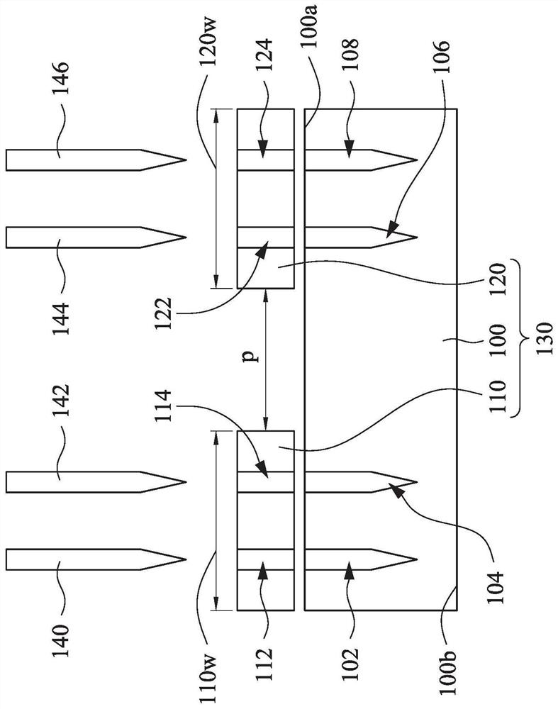
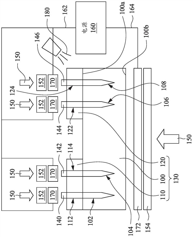
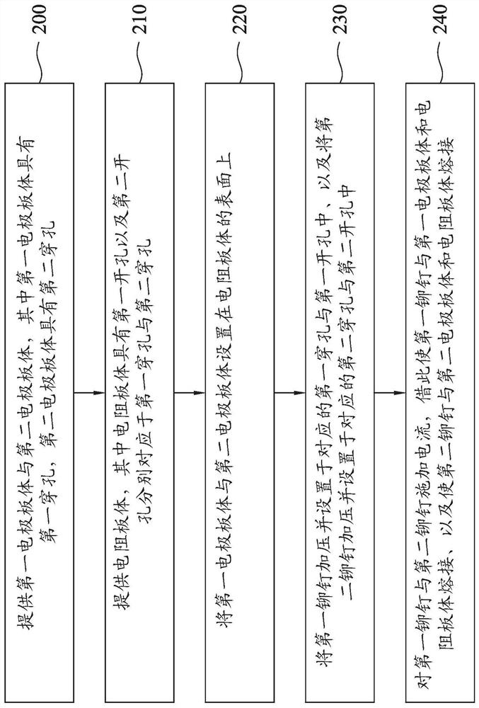
[0024] Please also refer to Figure 1A , Figure 1B and figure 2 ,in Figure 1A and Figure 1B It is a flow chart of a device for manufacturing shunt resistors according to the first embodiment of the present invention, figure 2 It is a flow chart of manufacturing a shunt resistor according to the first embodiment of the present invention. In this embodiment, when manufacturing the shunt resistor, step 200 is first performed to provide the first electrode plate body 110 and the second electrode plate body 120 . The first electrode plate body 110 has at least one first through hole, such as first through holes 112 and 114 . The second electrode plate body 120 has at least one second through hole, such as second through holes 122 and 124 . The first electrode plate body 110 and the second electrode plate body 120 can be formed into electrode plates with desired shapes and sizes by punching conductive electrode materials. The material of the first electrode plate body 110 ...


PUM


Abstract

A method for manufacturing a shunt resistor. In this method, a first electrode plate body and a second electrode plate body are provided. The first electrode plate body has a first through hole, and the second electrode plate body has a second through hole. A resistance plate body is provided, and the resistance plate body has a first opening and a second opening. The first electrode plate body and the second electrode plate body are arranged on the resistance plate body, and the first through hole is correspondingly located on the first opening, and the second through hole is correspondingly located on the second opening. The first rivet is pressed and arranged in the corresponding first through hole and the first opening, and the second rivet is pressed and arranged in the corresponding second through hole and the second opening. A current is applied to the first rivet and the second rivet, whereby the first rivet is welded to the first electrode plate body and the resistance plate body, and the second rivet is welded to the second electrode plate body and the resistance plate body. The welding method of using rivets to pre-position and directly applying current to the rivets can effectively improve production efficiency and greatly reduce the energy consumption of the welding resistor module.

Description

technical field [0001] The present invention relates to a resistor, and more particularly to a method of manufacturing a shunt resistor. Background technique [0002] When manufacturing shunt resistors, technologies such as E-beam welding, seam welding, or laser beam welding are generally used to combine high-conductivity electrode materials and resistance alloy materials, and Form a resistive composite. Cutting and punching the resistor composite material to form a plurality of preliminary models of the shunt resistors. Then, use the resistance adjustment machine to adjust the resistance value of the initial model of the shunt resistor, so as to make the resistance value of the shunt resistor more precise. [0003] However, the electron beam welding operation must be carried out under vacuum throughout, so the welding processing cost is high. In addition, material splashing is easy to occur during electron beam welding, which will not only affect the body of the resistan...

Claims


Application Information

Patent Timeline
Patent Type & Authority Patents(China)
IPC IPC(8): H01C17/00
CPCH01C17/00
Inventor 萧胜利林广成李焕文陈致龙
Owner YAGEO ELECTRONICS CHINA CO LTD
Learn More