An inner-column-outer-ring dual-zone composite solder joint structure and hybrid bonding method

A composite solder joint and core structure technology, applied in semiconductor/solid-state device components, semiconductor devices, electrical components, etc., can solve problems such as oxidation, chip failure surface, and inability to bond, so as to reduce process difficulty and save process cost , to avoid the effect of bonding failure

Inactive Publication Date: 2020-09-11
苏斯贸易(上海)有限公司
View PDF6 Cites 0 Cited by
  • Summary
  • Abstract
  • Description
  • Claims
  • Application Information

AI Technical Summary

Problems solved by technology

[0003] Excessively high bonding temperature may cause the wafer or substrate to be heated-cooled repeatedly during the multi-chip-to-wafer (substrate) bonding process, causing the chip to fail after repeated heating-cooling or the solder to be heated repeatedly Severe oxidation on the rear surface eventually leads to failure to bond

Method used


Image

  • An inner-column-outer-ring dual-zone composite solder joint structure and hybrid bonding method
  • An inner-column-outer-ring dual-zone composite solder joint structure and hybrid bonding method
  • An inner-column-outer-ring dual-zone composite solder joint structure and hybrid bonding method

Examples


Embodiment Construction

[0035] Specific embodiments of the present invention will be described in detail below.

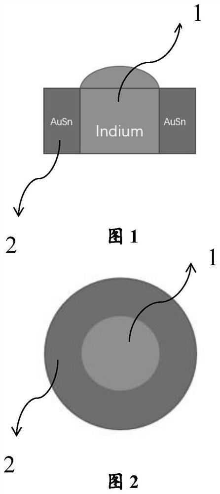
[0036] A double-zone composite solder joint structure with inner column and outer ring, such as Figure 1-2 As shown, it includes an inner core pillar 1 and a peripheral ring 2. The inner core pillar 1 uses metal indium, and the outer ring 2 uses a gold-tin alloy.

[0037] The method for preparing the above-mentioned inner column outer ring type double zone composite solder joint structure includes the following steps:

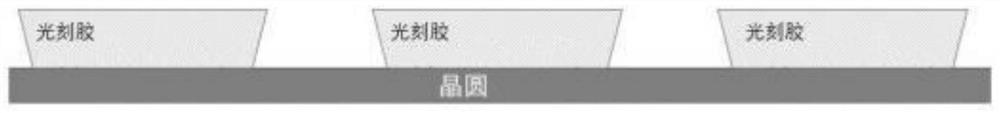
[0038] (1) Coating photoresist on the surface of the wafer, the thickness of the photoresist is 25μm;

[0039] (2) The wafer coated with photoresist in step (1) is sequentially exposed, developed and baked, and the resulting photoresist pattern has an inverted trapezoidal morphology on the surface of the wafer; image 3 Shown

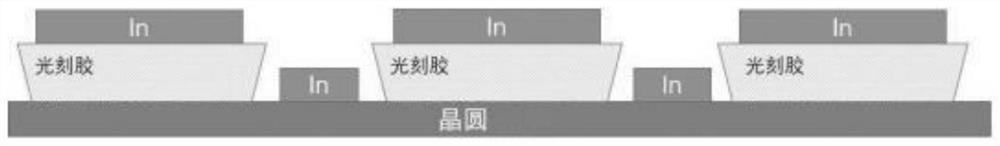
[0040] (3) Deposit metal indium on the surface of the photoresist pattern in step (2) by evaporation, and deposit metal indium on the surface of the wafer w...


PUM


Abstract

The invention discloses an inner-column outer-ring type double-zone composite solder joint structure which comprises a core column and a peripheral ring. The core column adopts a metal or metal systemwhich can be subjected to cold welding at room temperature, the peripheral ring is made of a high-temperature solder metal or metal system. The invention further discloses a hybrid bonding method based on the above solder joint structure. The method comprises the following steps of (1) providing a wafer (substrate) with the inner-column outer-ring type double-zone composite solder joint structure, (2) pre-bonding multiple chips to the wafer (substrate) one by one through a normal-temperature / low-temperature pressing mode, and (3) performing integral thermal compression bonding on the pre-bonded chips. According to the method, a bonding failure caused by a conventional multi-chip to single wafer (substrate) eutectic bonding process due to repeated heating is completely avoided, the overallefficiency of a process is greatly improved, the process difficulty in the chip preparation process is effectively reduced, and the process cost is greatly saved.

Description

Technical field [0001] The invention relates to the technical field of semiconductor manufacturing, in particular to an inner column outer ring type double-zone composite solder joint structure and a hybrid bonding method. Background technique [0002] At present, the commonly used multi-chip to single wafer or multi-chip to single substrate bonding technology usually uses only one metal solder combination. The commonly used solder combinations include gold-tin, silver-tin, copper-tin, tin-lead Etc., the required bonding temperature is usually between 200°C and 350°C. [0003] Too high bonding temperature may cause the wafer or substrate to be repeatedly heated and cooled during the multi-chip-to-wafer (substrate) bonding process, causing the chip to fail after repeated heating and cooling, or the solder to be heated repeatedly Severe oxidation on the back surface eventually leads to failure to bond. Summary of the invention [0004] The purpose of the present invention is to over...

Claims


Application Information

Patent Timeline
Patent Type & Authority Patents(China)
IPC IPC(8): H01L23/488H01L21/48H01L21/603
CPCH01L24/11H01L24/13H01L24/81H01L2224/113H01L2224/1147H01L2224/1162H01L2224/11849H01L2224/13014H01L2224/13018H01L2224/1302H01L2224/13109H01L2224/13111H01L2224/13116H01L2224/13139H01L2224/13144H01L2224/13147H01L2224/81203H01L2224/81H01L2224/95
Inventor 李震顾轶峰简·史蒂芬·莫泰龚里
Owner 苏斯贸易(上海)有限公司
Why Eureka
Try Eureka