Low-temperature polysilicon thin film transistor display panel and manufacturing method thereof

A technology of thin-film transistors and low-temperature polysilicon, which is applied in the direction of transistors, semiconductor/solid-state device manufacturing, and electric solid-state devices, and can solve problems such as reducing production capacity and increasing process time

Pending Publication Date: 2019-10-18
AU OPTRONICS KUNSHAN CO LTD
View PDF3 Cites 6 Cited by
  • Summary
  • Abstract
  • Description
  • Claims
  • Application Information

AI Technical Summary

Problems solved by technology

However, the increase in the thickness of the gate insulating layer will affect the depth

Method used


Image

  • Low-temperature polysilicon thin film transistor display panel and manufacturing method thereof
  • Low-temperature polysilicon thin film transistor display panel and manufacturing method thereof
  • Low-temperature polysilicon thin film transistor display panel and manufacturing method thereof

Examples


Embodiment Construction

[0025] Below in conjunction with accompanying drawing, structural principle and working principle of the present invention are specifically described:

[0026] The present invention provides a method for manufacturing a display panel, especially a method for manufacturing a low-temperature polysilicon thin film transistor in a display panel. For those skilled in the art, other structures adopt well-known manufacturing methods.

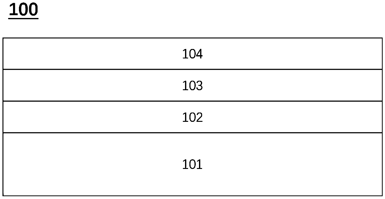
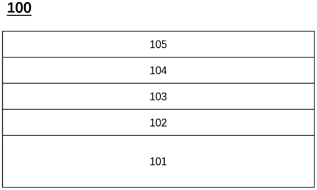
[0027] Figure 1A-Figure 1H It is a flowchart of a method for manufacturing a low-temperature polysilicon thin film transistor according to an embodiment of the present invention. The manufacturing method of the low temperature polysilicon thin film transistor 100 in this embodiment includes the following steps:

[0028] Such as Figure 1A As shown, a substrate 101 is firstly provided, wherein a buffer layer (not shown) can also be formed on the substrate 101, and a semiconductor layer 102 is formed on the substrate 101, and the semiconductor layer 10...


PUM


Abstract

The invention provides a low-temperature polysilicon thin film transistor display panel and a manufacturing method thereof. The manufacturing method comprises the steps: providing a substrate; forminga polysilicon layer, wherein the polysilicon layer is formed on the substrate; forming a first insulating layer, wherein the first insulating layer covers the polysilicon layer; forming a second insulating layer, wherein the second insulating layer covers the first insulating layer; forming a metal layer, wherein the metal layer is formed on the second insulating layer; patterning the metal layerand the second insulating layer so as to form a first patterned metal layer and a patterned second insulating layer; patterning the first patterned metal layer so as to form a second patterned metallayer; and injecting ions into the polysilicon layer so as to simultaneously form a heavily doped region and a lightly doped region.

Description

technical field [0001] The present invention relates to a display panel and a manufacturing method thereof, and in particular to a low-temperature polysilicon thin film transistor display panel and a manufacturing method thereof. Background technique [0002] With the development of technology, display devices are widely used in many electronic products, such as mobile phones, tablet computers, watches and so on. In order to improve display quality, large-size, high-resolution, high-brightness low-temperature polysilicon thin-film transistor display panels have emerged as the times require. [0003] In the existing low-temperature polysilicon thin film transistor display panel, generally when making a thin film transistor, ion implantation is usually performed after forming a gate metal layer to define a heavily doped region N+, forming a photoresist layer on the gate metal layer, and The gate metal layer is further etched to define a lightly doped region N−, and then ion i...

Claims


Application Information

Patent Timeline
IPC IPC(8): H01L21/336H01L29/786H01L27/12
CPCH01L29/66757H01L29/78675H01L27/1214
Inventor 陈峰毅
Owner AU OPTRONICS KUNSHAN CO LTD
Why Eureka
Try Eureka