Variable doped junction terminal preparation method

A technology of junction termination and variable doping, which is applied in the manufacture of semiconductor/solid-state devices, electrical components, circuits, etc., can solve the problems of increasing the number of ion implantations, achieve the effect of reducing the number of times and avoiding film thickness changes

Active Publication Date: 2016-08-31
NO 55 INST CHINA ELECTRONIC SCI & TECHNOLOGYGROUP CO LTD
View PDF6 Cites 6 Cited by
  • Summary
  • Abstract
  • Description
  • Claims
  • Application Information

AI Technical Summary

Problems solved by technology

But this method increases the number of ion implantations

Method used


Image

  • Variable doped junction terminal preparation method
  • Variable doped junction terminal preparation method
  • Variable doped junction terminal preparation method

Examples


Embodiment Construction

[0038] The technical solution of the present invention will be further elaborated below in conjunction with the accompanying drawings.

[0039] The invention discloses a method for preparing a variable doping junction terminal, comprising the following steps:

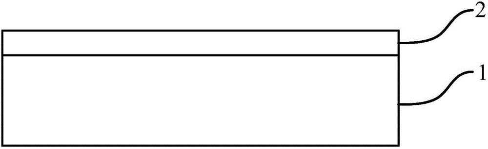
[0040] S1: grow the first dielectric layer 2 on the silicon carbide epitaxial layer 1, such as figure 1 shown;

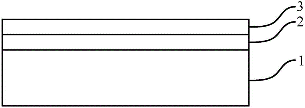
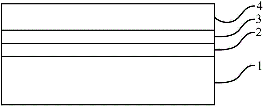
[0041] S2: growing the second dielectric layer 3 on the first dielectric layer 2, such as figure 2 As shown; the first etch barrier layer 4 is processed on the surface of the second dielectric layer 3, such as image 3 shown, and remove part of the first etch barrier layer 4 by etching, such as Figure 4 As shown, the unremoved first etch barrier layer 4 is still covering the second dielectric layer 3, and then the area not covered by the first etch barrier layer 4 in the second dielectric layer 3 is removed by etching, as Figure 5 As shown, the area covered by the first etch barrier layer 4 in the seco...


PUM


Abstract

The present invention discloses a variable doped junction terminal preparation method. An etching barrier layer is processed on the surface of a dielectric layer to form an echelonment medium morphology and then form the junction terminal of a grading structure through ion implantation. Through strictly controlling the etching speed ratio of two layers of medium, the variable doped junction terminal preparation method realizes step height accurate control and avoids the injection medium film thickness changing caused by etching ratio drifting. The injection dosage of each area of the junction terminal may be accurately controlled, and the number of times of ion injection in the device processing is reduced.

Description

technical field [0001] The invention relates to the field of semiconductor devices, in particular to a method for preparing variable doping junction terminals. Background technique [0002] SiC materials have large bandgap width, high breakdown electric field, high saturation drift velocity and high thermal conductivity. The superior properties of these materials make them ideal materials for making high-power, high-frequency, high-temperature-resistant, and radiation-resistant devices. The advantage of silicon carbide lies in the production of high-voltage devices, so in order to give full play to its material advantages, the terminal protection efficiency must be improved as much as possible. [0003] The theoretical protection efficiency in the form of junction termination protection is very high, and the blocking voltage of silicon carbide devices using junction termination protection can approach the theoretical limit. However, the junction terminal protection efficien...

Claims


Application Information

Patent Timeline
Patent Type & Authority Applications(China)
IPC IPC(8): H01L21/02H01L21/266
CPCH01L21/02356H01L21/266
Inventor 黄润华柏松陶永洪汪玲
Owner NO 55 INST CHINA ELECTRONIC SCI & TECHNOLOGYGROUP CO LTD
Why Eureka
Try Eureka