Multi-ADC synchronization device based on phase-locked delay
A synchronizing device and phase-locking technology, applied in the field of signal processing, can solve problems such as the adverse effects of stable reset of multi-channel ADCs, achieve flexible pulse generator functions, meet the requirements of low temperature drift performance, and reduce the number of uses
- Summary
- Abstract
- Description
- Claims
- Application Information
AI Technical Summary
Problems solved by technology
Method used
Image


Examples
Embodiment
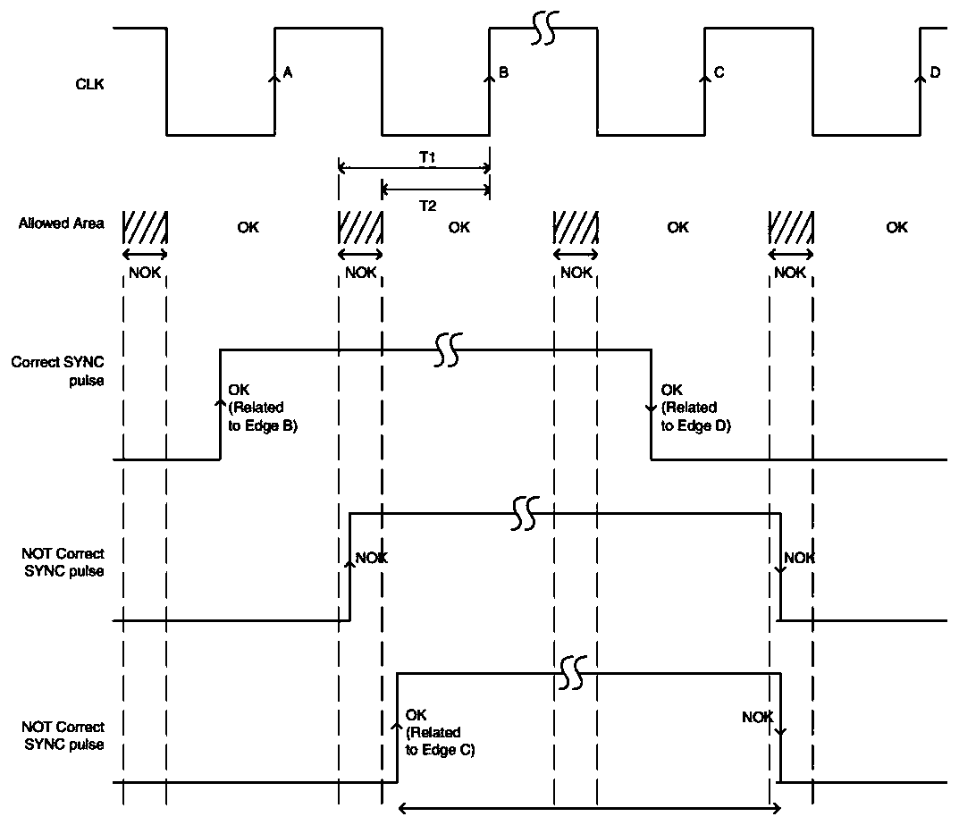
[0030] Figure 4 It is a schematic diagram of a multi-ADC synchronization device based on phase-locked delay in the present invention.
[0031] In this example, if Figure 4 As shown, the present invention is a multi-ADC synchronization device based on phase-locked delay, including: FPGA, clock generator, pulse generator and multi-chip ADC.
[0032] The FPGA is used to generate the clock synchronization signal SYNC and SPI control commands, then send the clock synchronization signal SYNC to the clock generator, and send the SPI control commands to the clock generator and the pulse generator at the same time.
[0033] The clock generator and the pulse generator adopt a double-cascaded phase-locked loop structure, and the connection mode of the clock tree structure is adopted between the two;
[0034] The double-cascaded phase-locked loop structure includes a first-stage phase-locked loop and a second-stage phase-locked loop, and each stage of the phase-locked loop is composed...
example
[0059] The clock generator of the present invention selects HMC7044 of ADI Company, and the pulse generator selects HMC7043 of ADI Company. Both devices have similar features and can be configured for device clock or SYSREF pulse mode. HMC7044 / 7043 provides 14 output channels with a maximum output frequency of 3.2GHz. It also has the functions of channel frequency division, delay and synchronization. The output level standard supports LVDS, LVPECL, CML and LVCMOS. In addition, the output delay of the HMC7044 / 7043 clock or pulse is less affected by temperature, such as Figure 7 shown. The analog delay step value of the clock chip is 25ps. As the delay of the analog delay increases, the influence of temperature increases accordingly. From -40 degrees Celsius to 85 degrees Celsius, the delay effect does not exceed 100ps, which has a greater performance improvement than previous methods. Therefore, the performance index of the HMC7044 / 7043 meets the design requirements of the ...
PUM
 Abstract
Description
Claims
Application Information