
Eureka
For R&D, Eureka makes reading and utilizing patents & technical documents easy.
Eureka AIR
Designed for self-driven R&D workflows. Generate viable solutions, solve complex R&D challenges, empower your innovation with AI.

Eureka Materials
Designed for material experts only. Revolutionize your material R&D, from search, analyze, to developing new materials.

TechResearch
Generate reliable direction feasibility study reports for your R&D in just a few steps.

TechSeek
Discover and master advanced knowledge NOW. Basics, ideas, possibilities, all at once.

TechMind
As an expert in R&D Theories, TechMind can generates customized viable solutions instantly.

TechRisk
Analyze your overall solution with one click, know your potential R&D risks in advance.

TechMonitor
Get weekly tech updates, stay abreast of the latest tech innovations and key insights.
Optical integrated circuits
An integrated circuit and optical technology, applied in the field of optical integrated circuits, can solve the problem of high optical loss of optical devices
- Summary
- Abstract
- Description
- Claims
- Application Information
AI Technical Summary
Problems solved by technology
Method used
Image

Examples
Embodiment Construction
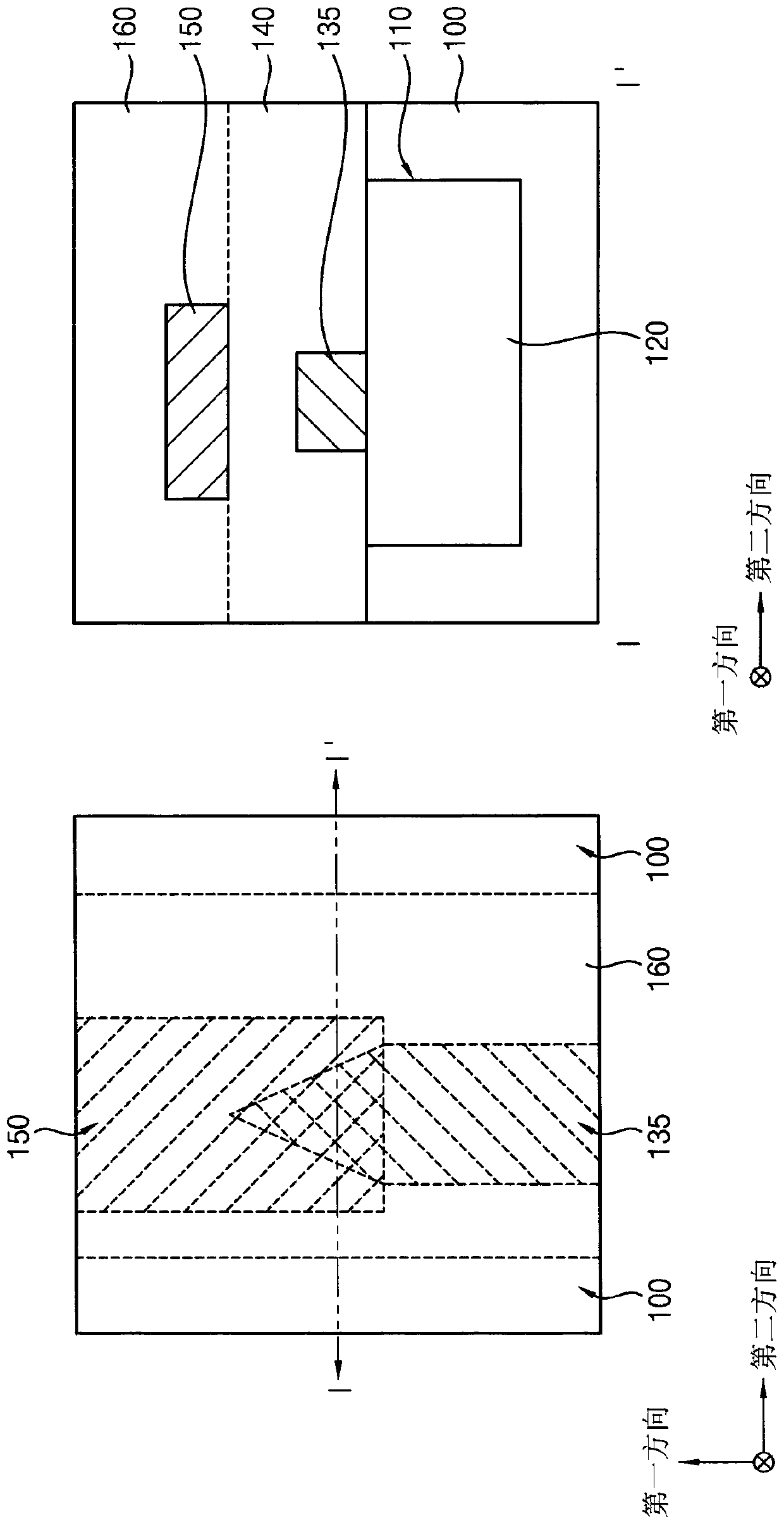
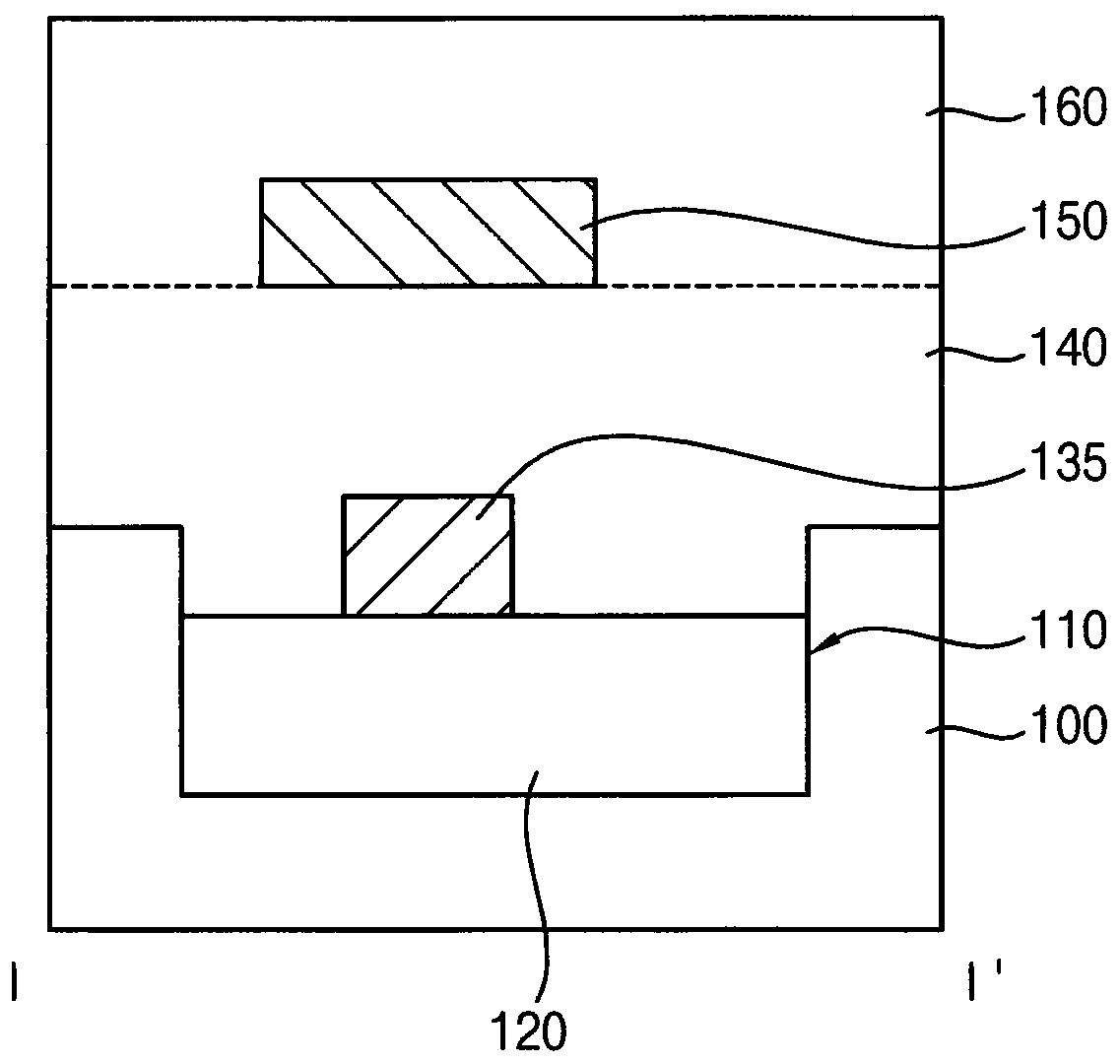
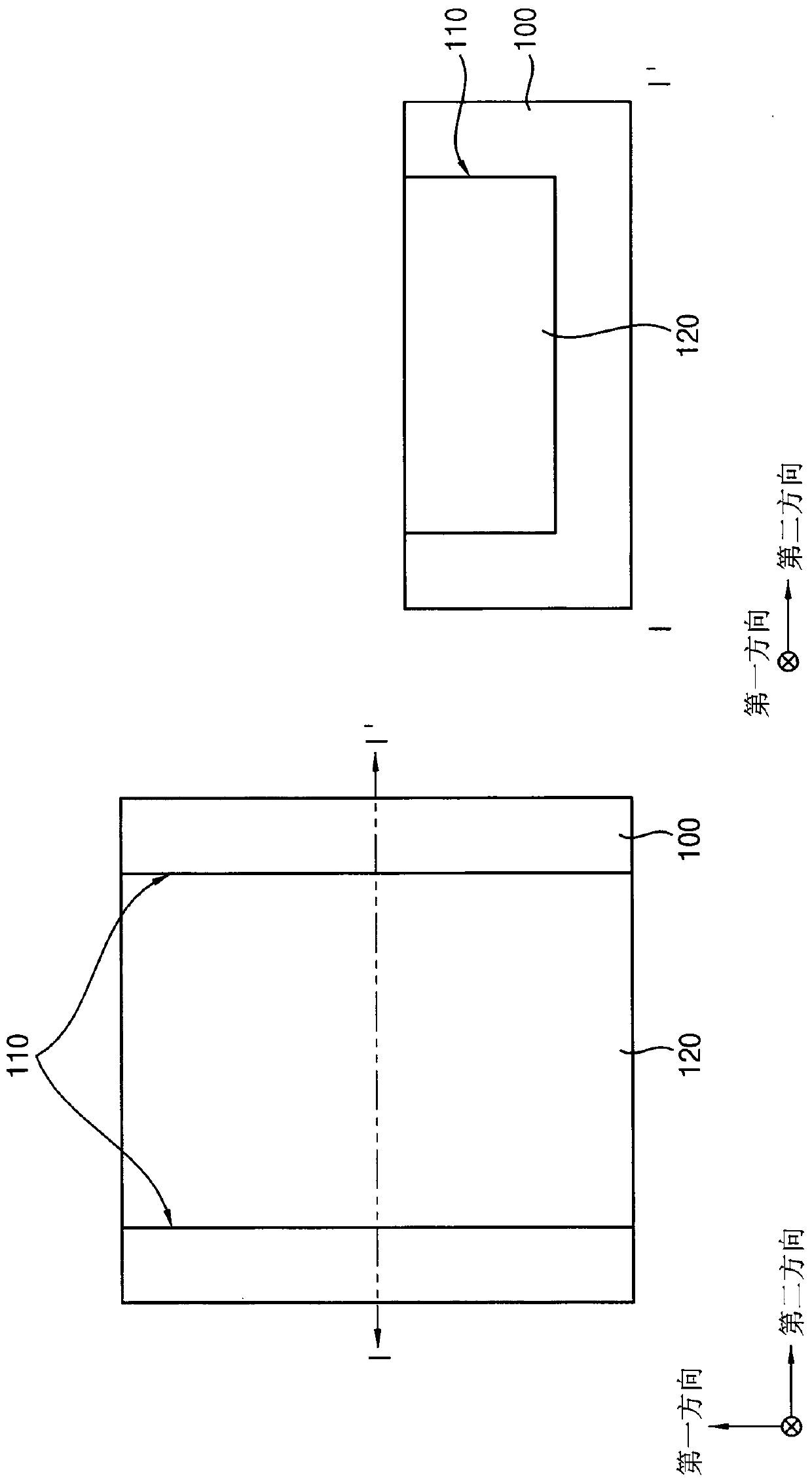
[0018] Example embodiments will be more clearly understood from the following detailed description taken in conjunction with the accompanying drawings.
[0019] Figure 1A including plan and cross-sectional views illustrating optical integrated circuits according to example embodiments, Figure 1B is a cross-sectional view illustrating an optical integrated circuit according to example embodiments. Each of the cutaway views is along the Figure 1A Intercepted on line II' in the plan view.
[0020] refer to Figure 1A , the optical integrated circuit may include: a first cladding layer 120 located in the trench 110 on / in the substrate 100; a first core 135 located on the first cladding layer 120; a second cladding layer 140 located between the substrate 100 and the first The cladding 120 is positioned on the first core 135 (for example, covers the first core 135); the second core 150 is on the second cladding 140 along the vertical direction substantially perpendicular to the ...
PUM
 Abstract
Description
Claims
Application Information
 - R&D Engineer
- R&D Manager
- IP Professional
- Industry Leading Data Capabilities
- Powerful AI technology
- Patent DNA Extraction
Browse by: Latest US Patents, China's latest patents, Technical Efficacy Thesaurus, Application Domain, Technology Topic, Popular Technical Reports.
© 2024 PatSnap. All rights reserved.Legal|Privacy policy|Modern Slavery Act Transparency Statement|Sitemap|About US| Contact US: help@patsnap.com