

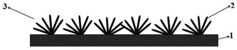
A copper indium gallium sulfur two-dimensional nanostructure array and its preparation method and application
A two-dimensional nanostructure, copper indium gallium sulfide technology, applied in nanotechnology, nano optics, nanotechnology, etc., can solve the problems of insufficient absorption, sensitivity to light incident angle, and high preparation cost
- Summary
- Abstract
- Description
- Claims
- Application Information
AI Technical Summary
Problems solved by technology
Method used
Image

Examples
Embodiment 1
[0034] A copper indium gallium sulfur two-dimensional nanostructure array, the preparation method of which comprises the following steps:
[0035] (1) Clean the FTO glass substrate sequentially with 1mol / L NaOH, 1mol / L HCl solution, absolute ethanol, and deionized water, and then put it into the bottom of the stainless steel reactor. Copper chloride dihydrate, thiourea and polyvinylpyrrolidone (PVP) are dissolved in 95% (v / v) ethanol (precursor liquid), put into reactor, the ratio of precursor liquid volume and reactor volume is 3:5 ;
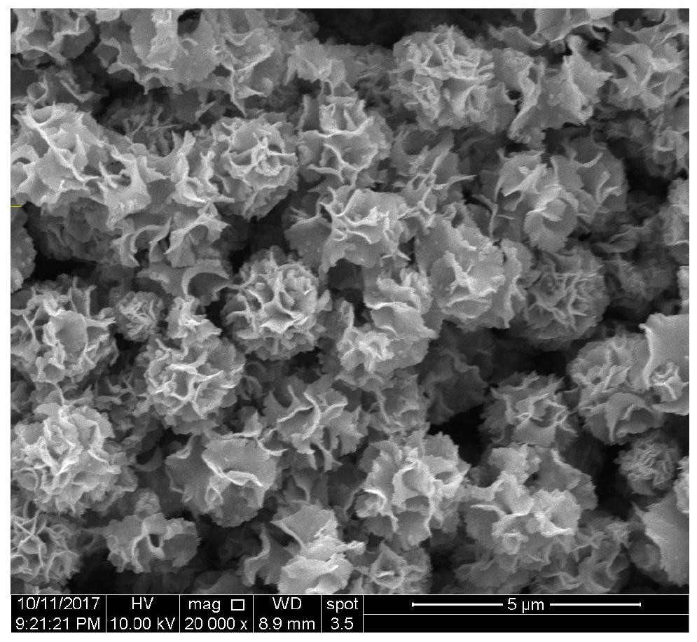
[0036] (2) After sealing the reaction kettle, put it into a blast drying oven, heat it at 100°C for 5h, take out the FTO glass substrate, wash and dry it, and obtain Cu substrates arranged regularly. 2 S nanosheet clusters;
[0037] (3) Through the continuous ion layer adsorption and reaction method (SILAR), in a constant temperature water bath at 10 ° C, the FTO glass substrate obtained in step (2) was sequentially placed in 0.1M InCl 3 sol...
Embodiment 2
[0040] A copper indium gallium sulfur two-dimensional nanostructure array, the preparation method of which comprises the following steps:
[0041] (1) Clean the FTO glass substrate sequentially with 1mol / L NaOH, 1mol / L HCl solution, absolute ethanol, and deionized water, and put it into the bottom of the stainless steel reactor. Copper chloride dihydrate, thiourea and polyvinylpyrrolidone (PVP) are dissolved in 95% (v / v) ethanol (precursor liquid), put into reactor, the ratio of precursor liquid volume and reactor volume is 4:5 ;
[0042] (2) After sealing the reaction kettle, put it into a blast drying oven, heat it at 300°C for 72h, take out the FTO glass substrate, wash and dry it, and obtain Cu substrates arranged regularly. 2 S nanosheet clusters;
[0043] (3) Through the continuous ion layer adsorption and reaction method (SILAR), in a constant temperature water bath at 20 ° C, the FTO glass substrate obtained in step (2) was sequentially placed in 0.5M InCl 3 solutio...
Embodiment 3
[0046] A copper indium gallium sulfur two-dimensional nanostructure array, the preparation method of which comprises the following steps:
[0047] (1) Clean the FTO glass substrate sequentially with 1mol / L NaOH, 1mol / L HCl solution, absolute ethanol, and deionized water, and then put it into the bottom of the stainless steel reactor. Copper chloride dihydrate, thiourea and PVP are dissolved in 95% ethanol (precursor solution), and put into a reactor, the ratio of the volume of the precursor solution to the volume of the reactor is 3:5;
[0048] (2) After sealing the reaction kettle, put it into a blast drying oven, heat it at 200°C for 24 hours, take out the FTO glass substrate, wash and dry it, and obtain Cu substrates arranged regularly. 2 S nanosheet clusters;
[0049] (3) Through the continuous ion layer adsorption and reaction method (SILAR), in a constant temperature water bath at 15 ° C, the FTO glass substrate obtained in step (2) was sequentially placed in 1M InCl 3...
PUM
| Property | Measurement | Unit |
|---|---|---|
| thickness | aaaaa | aaaaa |
| thickness | aaaaa | aaaaa |
| thickness | aaaaa | aaaaa |
Abstract
Description
Claims
Application Information