Super-surface array structure and application thereof in image display multiplexing
An array structure and image display technology, applied in the field of micro-nano optics, can solve the problems of high difficulty in metasurface control, difficult processing, complex nanoarray structure, etc., and achieve the effect of simple structure, easy processing, and low control difficulty
- Summary
- Abstract
- Description
- Claims
- Application Information
AI Technical Summary
Problems solved by technology
Method used
Image

Examples
Embodiment Construction
[0037] In order to better understand the above-mentioned technical solution, the above-mentioned technical solution will be described in detail below in conjunction with the accompanying drawings and specific implementation methods.
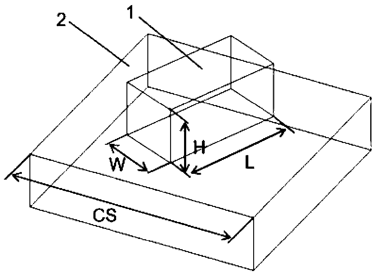
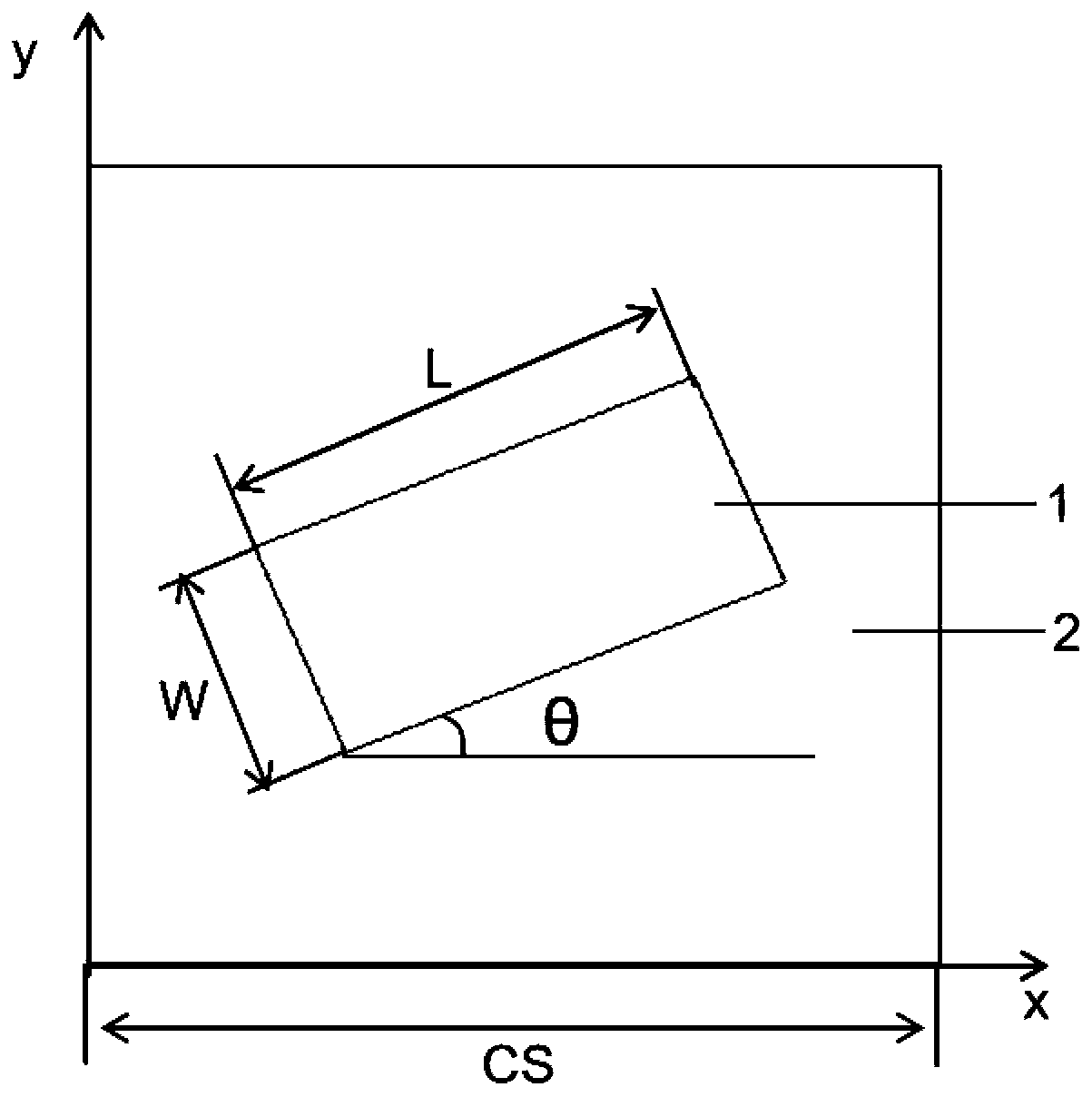
[0038] see Figure 1-Figure 2 , the present embodiment provides a metasurface array structure comprising: a substrate 2, on which a nanobrick array is arranged; The distances between the center points of adjacent nano-bricks 1 are the same; both the substrate 2 and the nano-bricks 1 are of sub-wavelength size, and the nano-bricks 1 are in the shape of a cuboid.
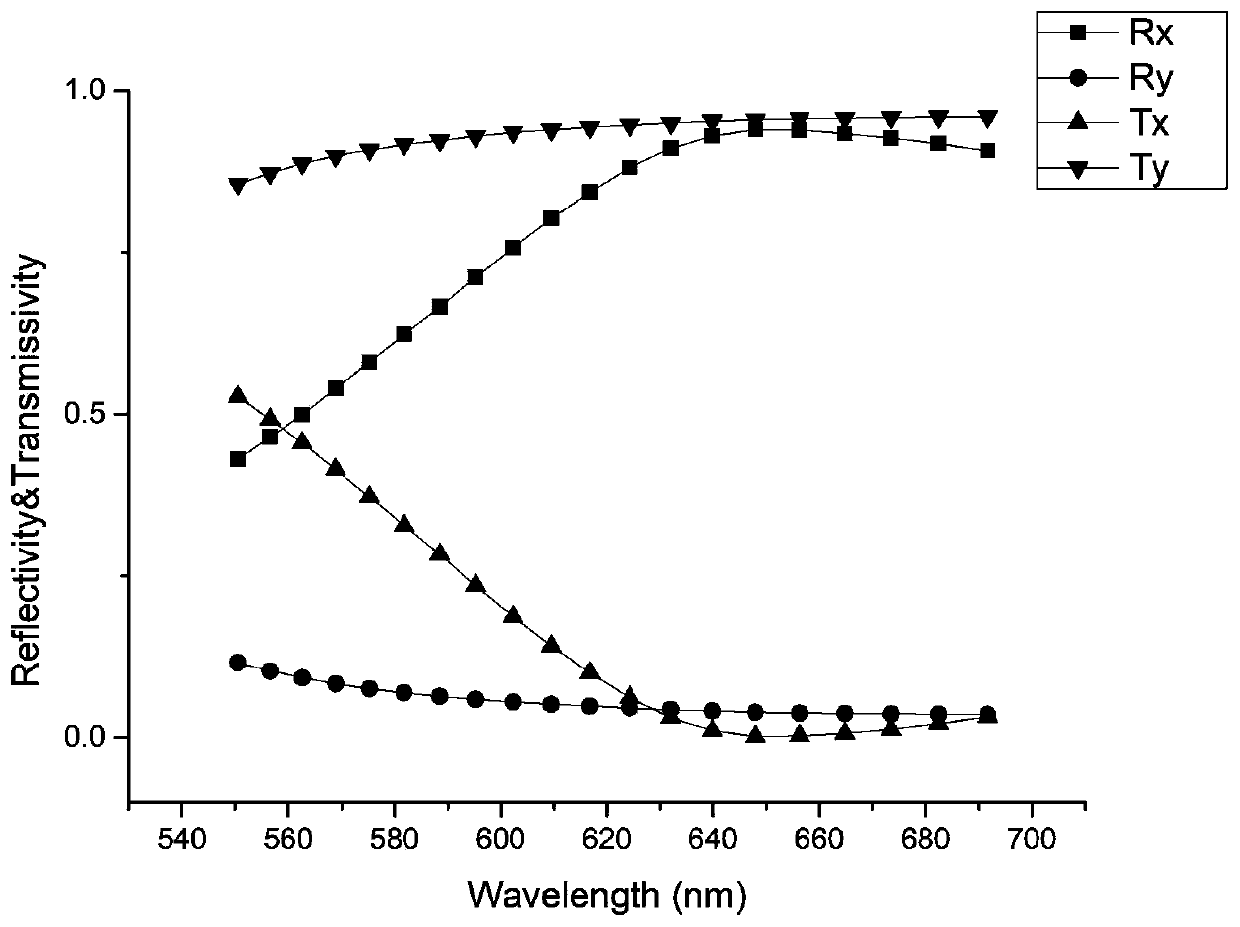
[0039] The size parameters of the nano-bricks are optimized by electromagnetic simulation software, and the optimized nano-brick array can realize the function of a micro-polarizer. Under the selected working wavelength, when the polarization direction of the incident ray polarization is along the long axis direction of the nano brick 1, the reflectivity is the highest; when the polariz...
PUM
| Property | Measurement | Unit |
|---|---|---|
| Length | aaaaa | aaaaa |
| Width | aaaaa | aaaaa |
| Height | aaaaa | aaaaa |
Abstract
Description
Claims
Application Information
 - Generate Ideas
- Intellectual Property
- Life Sciences
- Materials
- Tech Scout
- Unparalleled Data Quality
- Higher Quality Content
- 60% Fewer Hallucinations
Browse by: Latest US Patents, China's latest patents, Technical Efficacy Thesaurus, Application Domain, Technology Topic, Popular Technical Reports.
© 2025 PatSnap. All rights reserved.Legal|Privacy policy|Modern Slavery Act Transparency Statement|Sitemap|About US| Contact US: help@patsnap.com