

Electromigration test structure and method
A technology of test structure and test method, which is applied in the direction of semiconductor/solid-state device test/measurement, circuit, electrical components, etc. It can solve the problems of uniform heating of test metal wires, difficulty in providing target test temperature, etc., and achieve the effect of efficient conduction
- Summary
- Abstract
- Description
- Claims
- Application Information
AI Technical Summary
Problems solved by technology
Method used
Image

Examples
Embodiment Construction
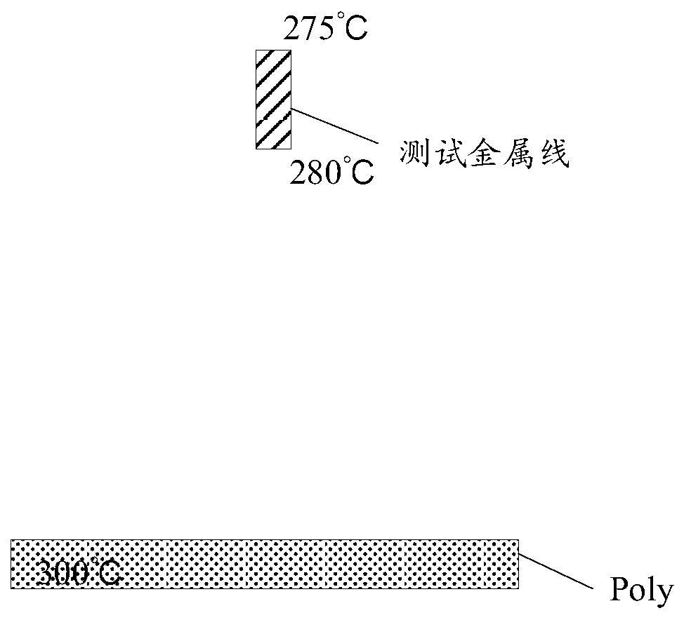
[0040] As mentioned in the background technology, when polysilicon wires are used for electromigration testing, the polysilicon heaters are generally arranged at the bottom layer. Due to the heat insulation effect of the interlayer medium and the dissipation effect of the heat transfer process, the temperature obtained by actually testing the metal wires is different from that of The temperatures produced by the polysilicon heaters are not equal and there will be a significant difference in the temperature at which the top and bottom of the test wires are heated.
[0041] For example, if figure 1 As shown, in the prior art, when a current is applied to the polysilicon wire poly to make the polysilicon wire poly generate a heating temperature of 300°C, due to the heat insulation effect of the interlayer dielectric and the dissipation effect of heat transfer, when reaching the metal test When the bottom of the metal test line is reached, the heating temperature may be reduced to...
PUM
 Abstract
Description
Claims
Application Information