Semiconductor device
A technology of semiconductor and paste, which is applied in the direction of semiconductor devices, semiconductor/solid-state device parts, amplifier parts, etc., and can solve problems such as difficult heat dissipation
- Summary
- Abstract
- Description
- Claims
- Application Information
AI Technical Summary
Problems solved by technology
Method used
Image

Examples
no. 1 example
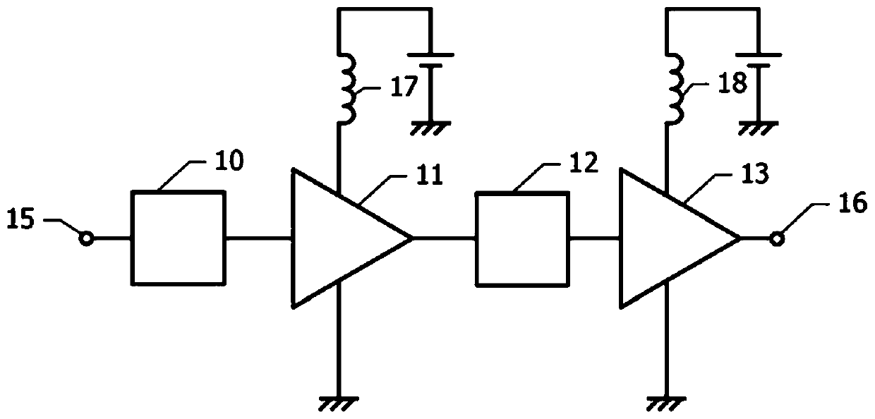
[0042] refer to Figure 1A ~ Figure 3 The accompanying drawings describe the semiconductor device of the first embodiment.
[0043] Figure 1A is a block diagram of the semiconductor device of the first embodiment. An input signal is input to the driver amplifier circuit 11 from the input terminal 15 via the impedance matching circuit 10 . The signal amplified by the driver stage amplifier circuit 11 is input to the output stage amplifier circuit 13 via the impedance matching circuit 12 . The signal amplified by the output stage amplifier circuit 13 is output from the output terminal 16 . DC power is supplied to the driver amplifier circuit 11 via the inductor 17 . DC power is supplied to the output stage amplifying circuit 13 via the inductor 18 .
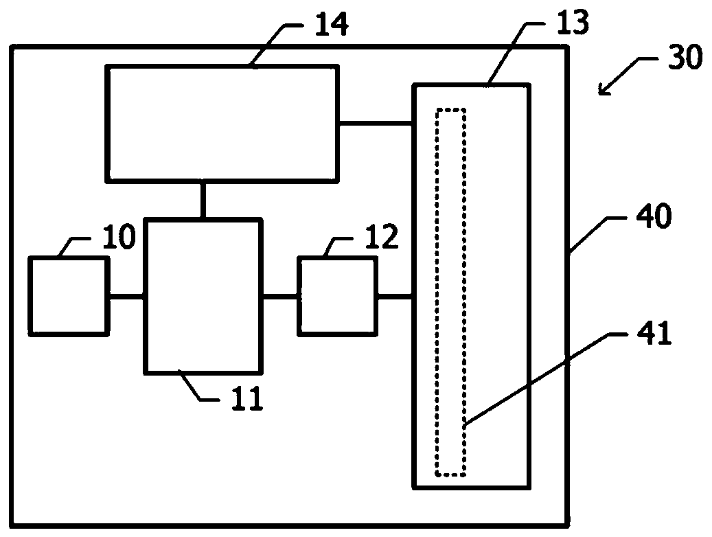
[0044] Figure 1B It is a plan view showing the layout of each circuit of the semiconductor chip 30 included in the semiconductor device of the first embodiment. Impedance matching circuits 10 and 12 , driver stage amplifier...
no. 2 example
[0073] Next, refer to Figure 4 The semiconductor device of the second embodiment will be described. Hereinafter, for the semiconductor device of the first embodiment ( Figure 1A ~ Figure 2B ) with the same configuration is omitted.
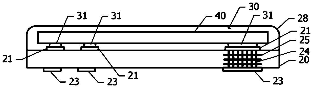
[0074] Figure 4 is a cross-sectional view of a semiconductor chip included in the semiconductor device of the second embodiment. In the first embodiment, the through via hole 41 ( Figure 2B ) side and bottom surface are covered by heat conduction member 51, and the remaining part in through hole 41 is hollow, or is sealed by resin ( Figure 1C )filling. In the second embodiment, a thermally conductive paste 49 is buried in the remaining part of the through via hole 41 . Here, “embedded” does not mean that the space inside the through via hole 41 is completely filled with the thermally conductive paste 49 . For example, even when the surface of the thermally conductive paste 49 is slightly dented, it can be called "embedding".
[0075] Th...
no. 3 example
[0079] Next, refer to Figure 5A as well as Figure 5B , the semiconductor device of the third embodiment will be described. Hereinafter, for the semiconductor device of the first embodiment ( Figure 1A ~ Figure 2B ) with the same configuration is omitted.
[0080] Figure 5A is the output stage amplifier circuit 13 formed on the semiconductor chip 30 included in the semiconductor device of the third embodiment ( Figure 1A ) top view. Figure 5B yes Figure 5A The sectional view on the dotted line 5B-5B. In the third embodiment, the recess 60 is formed on the bottom surface of the semiconductor substrate 40 . The concave portion 60 does not reach the upper surface of the semiconductor substrate 40 . In a plan view, the recess 60 at least partially overlaps the transistor 42 , and the through-hole 41 is disposed in the region of the recess 60 . exist Figure 5A In , an example in which the transistor 42 is arranged inside the concave portion 60 in plan view is shown....
PUM
 Abstract
Description
Claims
Application Information
 - R&D
- Intellectual Property
- Life Sciences
- Materials
- Tech Scout
- Unparalleled Data Quality
- Higher Quality Content
- 60% Fewer Hallucinations
Browse by: Latest US Patents, China's latest patents, Technical Efficacy Thesaurus, Application Domain, Technology Topic, Popular Technical Reports.
© 2025 PatSnap. All rights reserved.Legal|Privacy policy|Modern Slavery Act Transparency Statement|Sitemap|About US| Contact US: help@patsnap.com