Electroplated silicon wafer cleaning and drying device for integrated circuit board production

A technology of integrated circuit board and drying device, which is applied in the direction of drying gas layout, circuit, cleaning method using liquid, etc., to achieve the effect of improving work efficiency, improving cleaning and drying efficiency, and simple operation

Active Publication Date: 2019-11-05
深圳市荣之鑫科技有限公司
View PDF8 Cites 2 Cited by
  • Summary
  • Abstract
  • Description
  • Claims
  • Application Information

AI Technical Summary

Problems solved by technology

[0005] The object of the present invention is to provide a kind of electroplated silicon chip cleaning and drying device for integrated circuit board production, to solve the problems in the prior art

Method used


Image

  • Electroplated silicon wafer cleaning and drying device for integrated circuit board production
  • Electroplated silicon wafer cleaning and drying device for integrated circuit board production
  • Electroplated silicon wafer cleaning and drying device for integrated circuit board production

Examples


Embodiment Construction

[0037] The following will clearly and completely describe the technical solutions in the embodiments of the present invention with reference to the accompanying drawings in the embodiments of the present invention. Obviously, the described embodiments are only some, not all, embodiments of the present invention. Based on the embodiments of the present invention, all other embodiments obtained by persons of ordinary skill in the art without making creative efforts belong to the protection scope of the present invention.

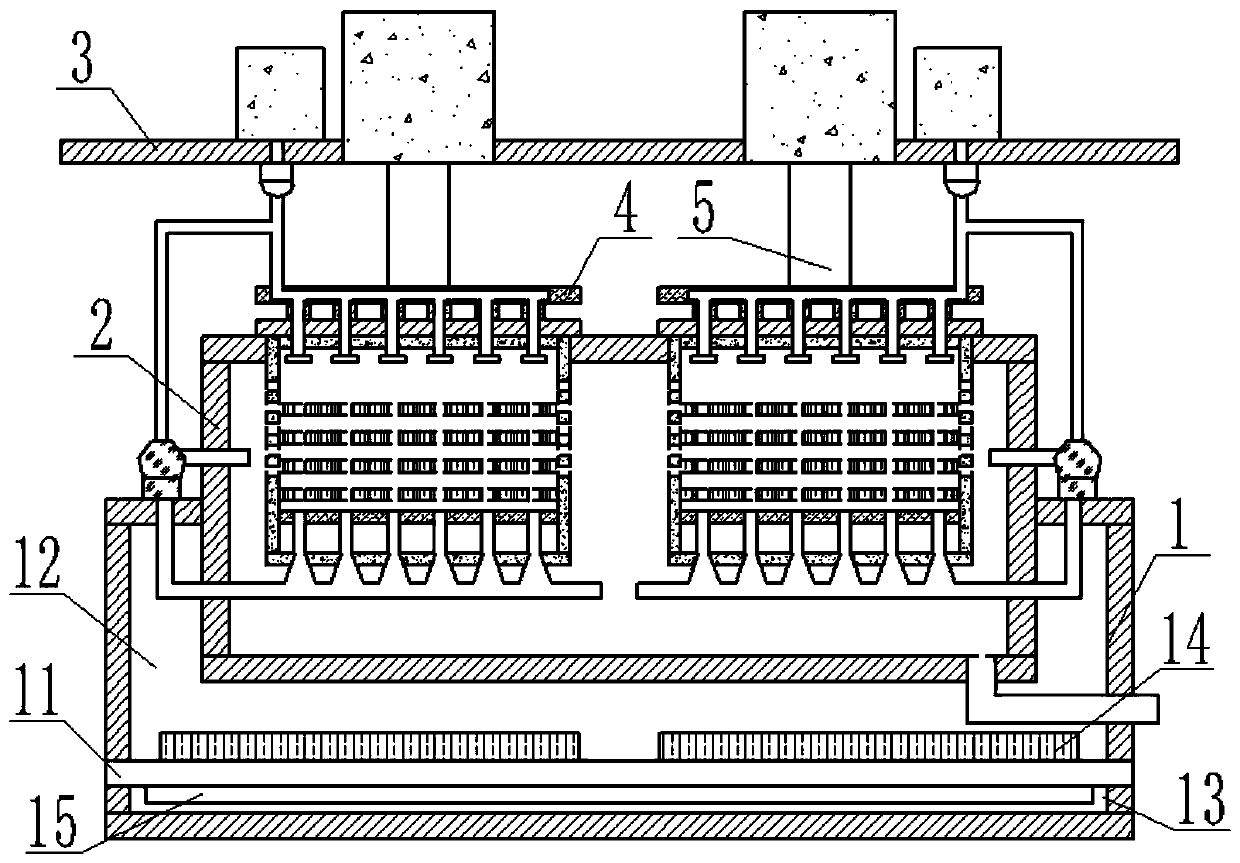
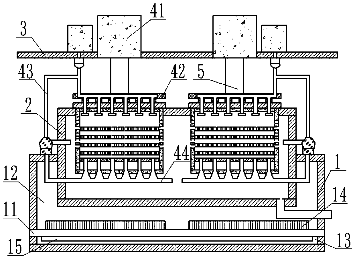
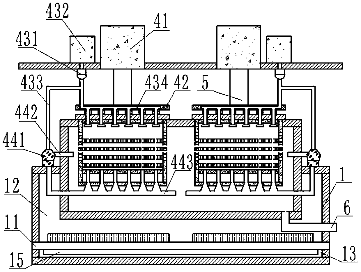
[0038] Such as Figure 1-Figure 6 As shown, a device for cleaning and drying electroplated silicon wafers for integrated circuit board production includes electroplated silicon wafers. The cleaning and drying device includes a holding tank 1, a cleaning tank 2 and several clamping devices. A partition 11, the partition 11 is arranged horizontally, and the partition 11 divides the space in the receiving tank 1 into an upper chamber 12 and a lower chamber 13, th...


PUM


Abstract

The invention discloses an electroplated silicon wafer cleaning and drying device for integrated circuit board production. The cleaning and drying device comprises an electroplated silicon wafer, andthe cleaning and drying device comprises a cleaning tank, an accommodating tank and a plurality of clamping devices, wherein a partition plate is arranged in the accommodating tank and divides the space in the accommodating tank into an upper cavity and a lower cavity, a plurality of vibrating parts are arranged on the partition plate, transferring water is contained in the upper cavity, and a vibrating plate is arranged in the lower cavity; the bottom end of the cleaning tank is located in the transferring water, a cleaning solution is contained in the cleaning tank, a mounting frame is arranged above the cleaning tank, the bottom ends of the clamping devices are located in the cleaning tank, and the top ends of the clamping devices are all connected with the mounting frame; and the electroplated silicon wafer is located in the clamping device. According to the device, the structure design is reasonable, the operation is simple, the cleaning and drying efficiency of the electroplatedsilicon wafer is effectively improved, the cleaning and drying effects of the electroplated silicon wafer are improved, meanwhile, the operation of the whole device is more flexible, and higher practicability is achieved.

Description

technical field [0001] The invention relates to the technical field of circuit board production, in particular to an electroplated silicon chip cleaning and drying device for integrated circuit board production. Background technique [0002] Circuit board, also called PCB board, makes the circuit miniaturized and intuitive, and plays an important role in mass production of fixed circuits and optimizing the layout of electrical appliances. The circuit board can be called a printed circuit board or a printed circuit board. The English name is (Printed Circuit Board) PCB, (Flexible Printed Circuit board) FPC circuit board (FPC circuit board is also called flexible circuit board). A highly reliable and excellent flexible printed circuit board made of polyester film. [0003] In the production process of circuit boards, generally we need to electroplate tin and nickel on silicon wafers, and the silicon wafers after electroplating need to be cleaned and dried. Nowadays, in the pr...

Claims


Application Information

Patent Timeline
IPC IPC(8): B08B3/12B08B3/02B08B13/00F26B21/00H01L21/67
CPCB08B3/12B08B3/02B08B13/00F26B21/004H01L21/67023H01L21/6704H01L21/67051
Inventor 郝建华李会斌李子考
Owner 深圳市荣之鑫科技有限公司
Why Eureka
Try Eureka