Width measuring method for nano-strip or nano-sheet of semiconductor device
A measurement method and nano-stripe technology, applied in measurement devices, instruments, etc., can solve the problems of general electrical yield connection, slow measurement speed, and small number of samples, and achieve fast test speed, good yield, and simple test. Effect
- Summary
- Abstract
- Description
- Claims
- Application Information
AI Technical Summary
Problems solved by technology
Method used
Image

Examples
Embodiment Construction
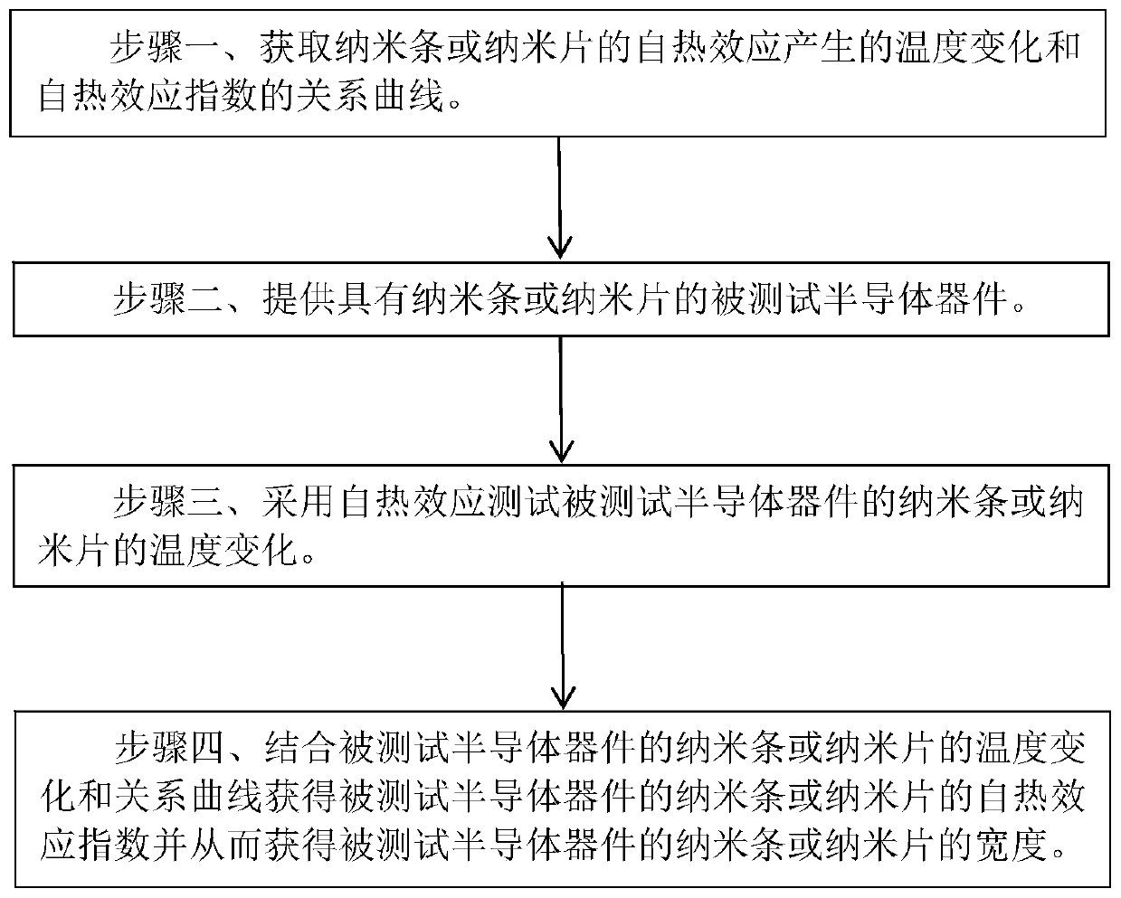
[0033] Such as figure 2 Shown is a flowchart of a method for measuring the width of a nanobar or a nanosheet of a semiconductor device according to an embodiment of the present invention; the method for measuring the width of a nanobar or a nanosheet of a semiconductor device according to an embodiment of the present invention includes the following steps:
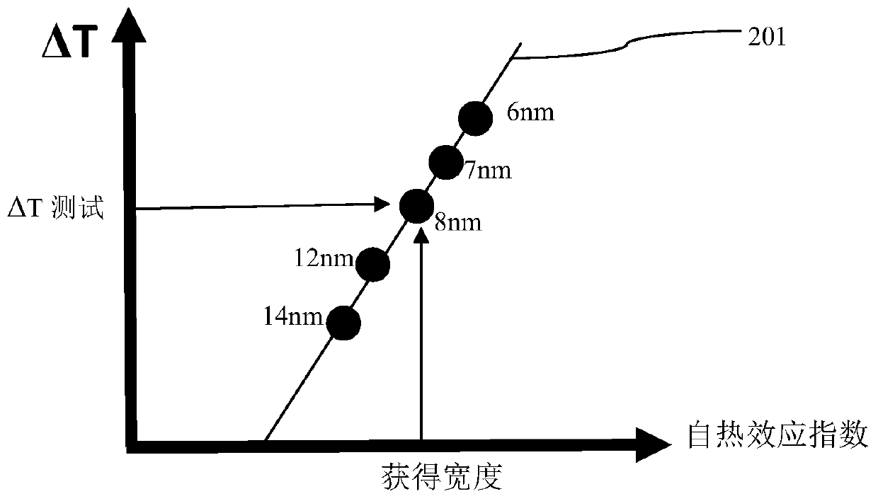
[0034] Step 1. Obtain a relationship curve between the temperature change caused by the self-heating effect of the nano-strips or nano-sheets and the self-heating effect index; the self-heating effect index is related to the height and width of the nano-strips or nano-sheets. The self-heating effect index is proportional to the ratio of the height and width of the corresponding nanorods or nanosheets.
[0035] In the embodiment of the present invention, the linear regression model in which the temperature change and the self-heating effect index have a linear relationship is obtained through the relationship curve; the re...
PUM
 Abstract
Description
Claims
Application Information