Contact unit structure and matrix probe card with same

A contact unit and probe card technology, which is used in the testing of single semiconductor devices, parts of electrical measuring instruments, measuring devices, etc. The effect of reducing parasitic inductance and shortening the distance between PADs

Active Publication Date: 2019-11-05
SHANGHAI HUALI MICROELECTRONICS CORP
View PDF16 Cites 0 Cited by
  • Summary
  • Abstract
  • Description
  • Claims
  • Application Information

AI Technical Summary

Problems solved by technology

The above situation has caused the limitation of the pendulum density of the existing probe card. In order to increase the test frequency, it is

Method used


Image

  • Contact unit structure and matrix probe card with same
  • Contact unit structure and matrix probe card with same
  • Contact unit structure and matrix probe card with same

Examples


Example Embodiment

[0045] Embodiments of the present invention are described below through specific specific examples, and those skilled in the art can fully understand other advantages and technical effects of the present invention from the content disclosed in this specification. The present invention can also be implemented or applied through different specific implementation modes, and various details in this specification can also be applied based on different viewpoints, and various modifications or changes can be made without departing from the general design idea of ​​the invention. It should be noted that, in the case of no conflict, the following embodiments and the features in the embodiments can be combined with each other.

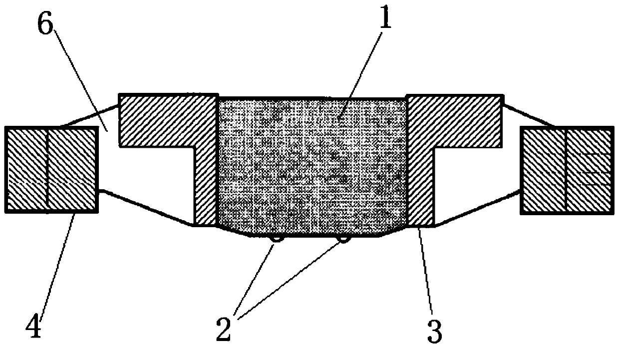
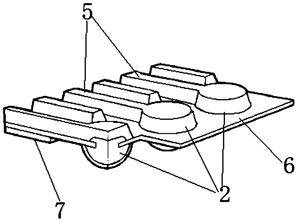
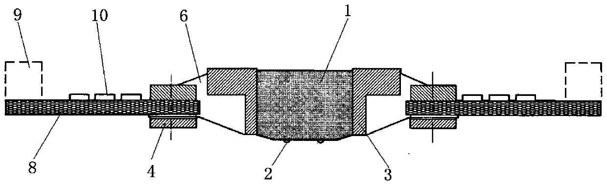
[0046] like figure 1 to combine figure 2 As shown, the present invention provides a feasible embodiment of the contact unit structure used for silicon chip level reliability testing, including: contact telescopic adjustment structure 1, contact metal bump 2, L...


PUM


Abstract

The invention discloses a contact unit structure for silicon chip level reliability test. The contact unit structure comprises a contact telescoping adjustment structure, first and second fixation members and first, second and third conductive connecting pieces; the contact telescoping adjustment structure is provided at least one contact in the bottom, andthe contact is electrically connected toor disengaged from a to-be-tested silicon chip; the first fixation members are arranged in the two sides of the contact telescoping adjustment structure respectively; the first conductive connecting piece electrically leads out the contact; the second conductive connecting piece is arranged under the first conductive connecting piece, and connected with the first fixation members outside the two sides of the contact telescoping adjustment structure; the third conductive connecting piece is arranged under the second conductive connecting piece, and the contact unit structure is connected to theground via the third conductive connecting piece; and the second fixation members are arranged outside the two sides of the second conductive connecting piece respectively, and the contact unit structure is fixedly to another external connecting structure via the second fixation members. The invention also discloses a matrix probe card with the contact unit structure. Thus, the contact pressure can be adjusted, different needs for test can be met, the parasitic inductance can be reduced, and the available frequency for test is improved.

Description

technical field [0001] The invention relates to the field of semiconductor testing, in particular to a contact unit structure for silicon chip testing. The present invention also relates to a matrix probe card having the contact unit structure. Background technique [0002] At present, silicon wafer-level probes often use cantilever needles and vertical probes. Existing silicon wafer-level reliability tests need to swing and adjust needles according to the measured object. For some chips with a large number of simultaneous tests, irregular placement of chip PADs, many PADs, or relatively small PAD spacing, it will be difficult to make probe cards, which is time-consuming and labor-intensive. And because there is a parasitic inductance of nearly 20nH in the probe, the test frequency of the general probe card can only be 50MHz. The above-mentioned situation causes the density of the swing pins of the existing probe card to be limited. In order to increase the test frequency,...

Claims


Application Information

Patent Timeline
IPC IPC(8): G01R1/073G01R1/04G01R31/26
CPCG01R1/0408G01R1/07314G01R31/2601
Inventor 武建宏
Owner SHANGHAI HUALI MICROELECTRONICS CORP
Why Eureka
Try Eureka