Display panel, display device and manufacturing method of display panel

A display panel and thickness direction technology, which is applied in the direction of electrical components, electric solid devices, circuits, etc., can solve the problems of poor brightness uniformity and uneven current distribution of the display panel, so as to avoid poor contact, improve brightness uniformity, and smooth surface Effect

Active Publication Date: 2019-11-05
CHENGDU VISTAR OPTEOLECTRONICS CO LTD
View PDF3 Cites 11 Cited by
  • Summary
  • Abstract
  • Description
  • Claims
  • Application Information

AI Technical Summary

Problems solved by technology

However, the existing common cathode connection scheme has the problem of un

Method used


Image

  • Display panel, display device and manufacturing method of display panel
  • Display panel, display device and manufacturing method of display panel
  • Display panel, display device and manufacturing method of display panel

Examples


Embodiment Construction

[0034]The present invention will be further described in detail below in conjunction with the accompanying drawings and embodiments. It should be understood that the specific embodiments described here are only used to explain the present invention, but not to limit the present invention. In addition, it should be noted that, for the convenience of description, only some structures related to the present invention are shown in the drawings but not all structures.

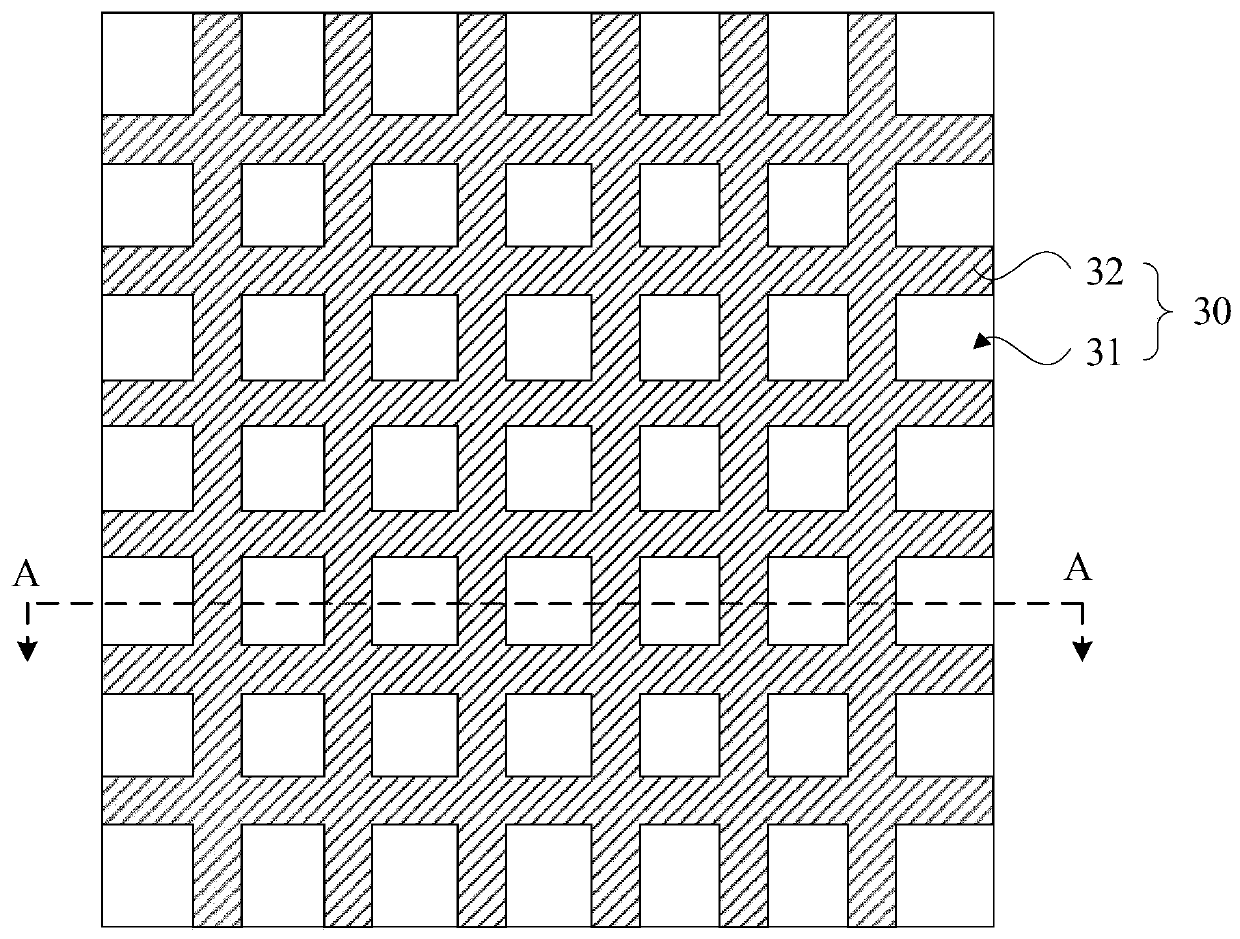
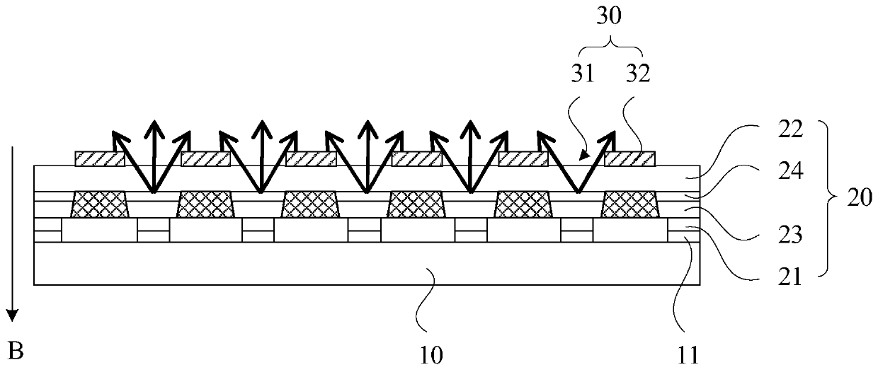
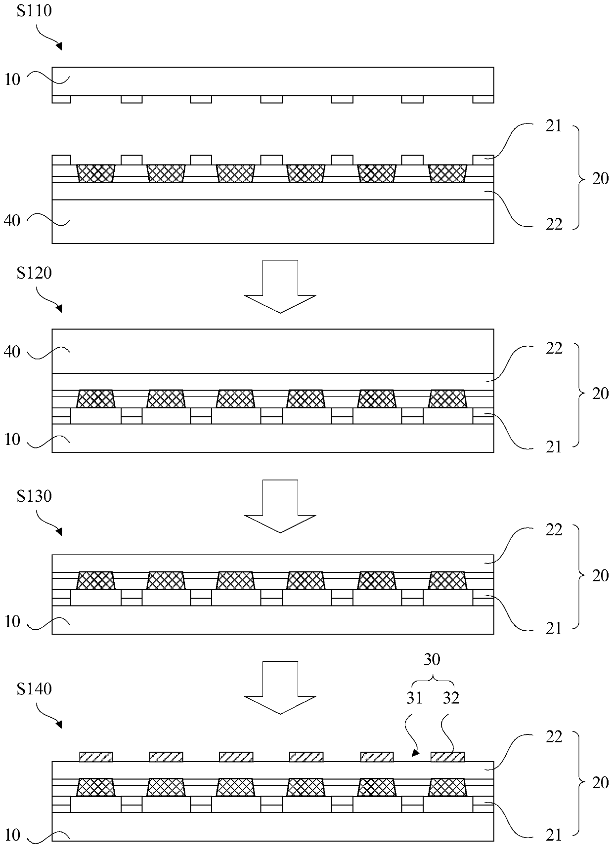
[0035] figure 1 It is a schematic top view structural diagram of a display panel provided by an embodiment of the present invention, figure 2 along figure 1 Schematic diagram of the cross-sectional structure of A-A. see figure 1 and figure 2 , the display panel includes: at least one LED chip 20 and a conductive layer 30 . The light emitting diode chip 20 includes a first electrode 21 and a first semiconductor layer 22 which are stacked. The conductive layer 30 is located on a side of the LED chip 20 away f...


PUM


Abstract

The embodiment of the invention discloses a display panel, a display device and a manufacturing method of the display panel. The display panel comprises at least one light emitting diode chip and a conducting layer, wherein the light emitting diode chip comprises a first electrode and a first semiconductor layer which are arranged in a laminated manner; the conducing layer is positioned at one side, which is away from a first electrode, of the light emitting diode chip; the conducting layer is in contact with the first semiconductor layer; and the conducting layer comprises a hollowed-out part, and the projection of the hollowed-out part on the conducting layer is overlapped with the projection of the first electrode on the conducting layer in the thickness direction of the first semiconductor layer. The embodiment of the invention achieves the effect of reducing the resistance of the current conducting layer with low process difficulty on the basis of ensuring the light emitting rateof the display panel.

Description

technical field [0001] The embodiments of the present invention relate to the field of display technology, and in particular, to a display panel, a display device, and a method for manufacturing the display panel. Background technique [0002] Micro Light Emitting Diode (micro-LED / μLED) display panels integrate light emitting diode (Light Emitting Diode, LED) chips with a size of less than 100 microns on a substrate as display pixels to realize image display. Each display pixel can be addressed and individually driven to light up, so the Micro-LED display panel is a self-illuminating display panel. [0003] In the prior art, the LED chip adopts the solution of the current conduction layer to realize the common cathode connection, and the current conduction layer conducts and distributes the current conduction to each LED chip (pixel) in the display area. However, the existing common cathode connection scheme has the problems of uneven current distribution and poor brightnes...

Claims


Application Information

Patent Timeline
IPC IPC(8): H01L27/15H01L33/00H01L33/38H01L33/60
CPCH01L27/156H01L33/0095H01L33/385H01L33/60H01L25/0753H01L33/04
Inventor 杨婷慧王雪丹
Owner CHENGDU VISTAR OPTEOLECTRONICS CO LTD
Why Eureka
Try Eureka