Display substrate, preparation method thereof, and display device

A technology for display substrates and driving substrates, which is applied in the fields of semiconductor/solid-state device manufacturing, semiconductor devices, electrical components, etc., can solve the problems of low efficiency of Micro-LED, excessive amount of solder paste, low yield, etc., to avoid N pole The effect of short circuit with P pole

Active Publication Date: 2019-11-05
BOE TECH GRP CO LTD
View PDF11 Cites 25 Cited by
  • Summary
  • Abstract
  • Description
  • Claims
  • Application Information

AI Technical Summary

Problems solved by technology

When using solder paste to bind Micro-LEDs, it is easy to cause too much solder paste, which leads to a short circuit between the N

Method used


Image

  • Display substrate, preparation method thereof, and display device
  • Display substrate, preparation method thereof, and display device
  • Display substrate, preparation method thereof, and display device

Examples


no. 1 example

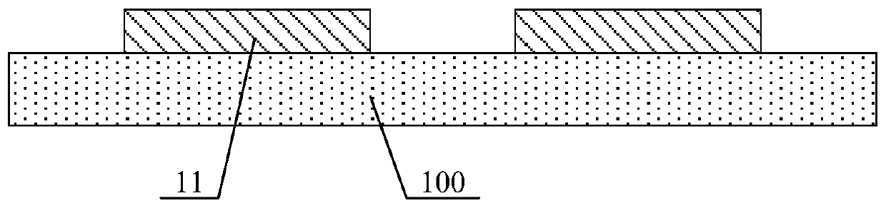
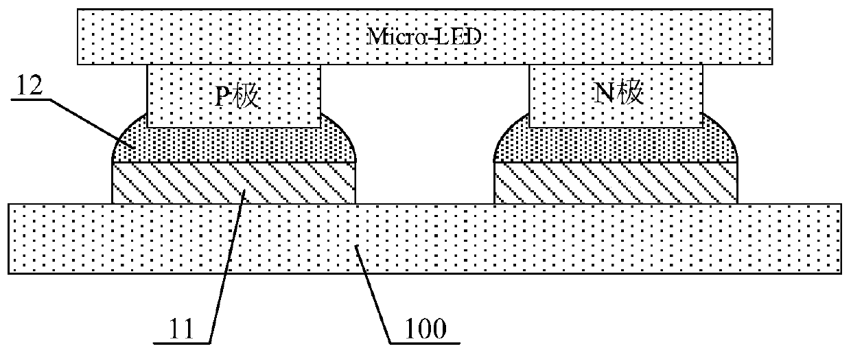
[0069] figure 2 A schematic structural diagram of the substrate is shown for the first embodiment of the present invention. Such as figure 2 As shown, the display substrate includes a driving substrate 100 and a bonding pad 11 disposed on the driving substrate 100 , and the bonding pad 11 is electrically connected to the driving substrate 100 . The display substrate further includes an insulating structure layer 21 disposed on the welding pad 11 , and the insulating structure layer 21 is provided with a groove 22 exposing the welding pad 11 . Binding material 23 is accommodated in the groove 22 , and the pins of the micro LEDs are electrically connected to the welding pads 23 through the binding material 23 .

[0070] In the display substrate of the embodiment of the present invention, when the Micro-LED is bound and connected to the display substrate, the dispenser can be controlled to place the binding material such as solder paste in the groove 22, and the groove 22 can...

no. 2 example

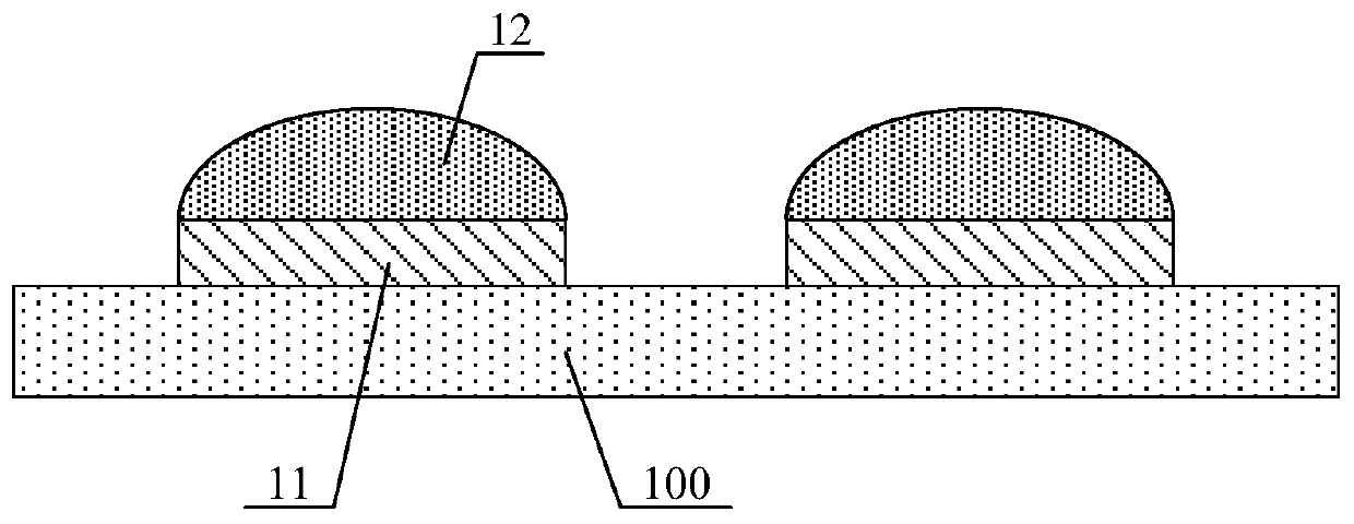
[0092] Figure 4A schematic structural diagram of the substrate is shown for the second embodiment of the present invention. The difference from the first embodiment is that if Figure 4 As shown, in this embodiment, the display substrate further includes a metal connection layer 24 disposed in the groove 22 , the metal connection layer 24 is in contact with both the bottom surface and the side surface of the groove, and the metal connection layer 24 is electrically connected to the welding pad 11 . The inner side of the metal connection layer 24 forms a sub-groove 25 corresponding to the groove 22, and the binding material is accommodated in the sub-groove 25, and the micro light-emitting diode is electrically connected to the metal connection layer 24 through the binding material 23, and then electrically connected to the welding pad. connect.

[0093] In the display substrate of the embodiment of the present invention, when the binding material 23 is dotted into the sub-g...

no. 3 example

[0126] Based on the inventive concepts of the aforementioned embodiments, an embodiment of the present invention further provides a display device, which includes the display substrate using the aforementioned embodiments. The display device can be any product or component with a display function such as a mobile phone, a tablet computer, a television, a monitor, a notebook computer, a digital photo frame, a navigator, and the like.


PUM

PropertyMeasurementUnit
Depthaaaaaaaaaa
Thicknessaaaaaaaaaa
Thicknessaaaaaaaaaa

Abstract

The invention discloses a display substrate, a preparation method thereof and a display device. The display substrate includes a driving substrate and a welding pad disposed on the driving substrate.The welding pad is electrically connected to the driving substrate. The display substrate further includes an insulating structural layer disposed on the welding pad, the insulating structural layer is provided with a recess exposing the welding pad, a binding material is received in the recess, and a Micro-LED is electrically connected to the welding pad through the binding material. According tothe display substrate, when the Micro-LED is electrically connected to the display substrate, a dispenser can be controlled to dispense the binding material such as solder paste into the recess, therecess can restrict the binding material from flowing during the binding process, and therefore, the short-circuit of an N-pole and a P-pole of the Micro-LED caused by excessive dispensing can be avoided.

Description

technical field [0001] The invention relates to the field of display technology, in particular to a display substrate, a preparation method thereof, and a display device. Background technique [0002] Micro-LED display is to shrink the size of the existing LED to less than 100μm, making the size of the LED about 1% of the size of the existing LED, and then through the mass transfer technology, the micron-scale R, G, B Three-color Micro-LEDs are transferred to the driving substrate to form Micro-LED displays of various sizes. To put it simply, Micro-LED is the thinning, miniaturization and arraying of LEDs. Each Micro-LED pixel can be addressed and driven to emit light independently, and the distance between adjacent pixels is reduced from millimeters to microns. Micro-LED has many advantages such as self-illumination, high brightness, high contrast, ultra-high resolution and color saturation, long life, fast response, energy saving, and wide adaptability to environments. M...

Claims


Application Information

Patent Timeline
IPC IPC(8): H01L27/15H01L33/00H01L33/62H01L21/60
CPCH01L27/15H01L33/0095H01L33/62H01L24/83H01L2224/832H01L25/167H01L2933/0066H01L27/156H01L33/56H01L2933/005
Inventor 梁志伟罗雯倩刘英伟曹占锋王珂
Owner BOE TECH GRP CO LTD
Why Eureka
Try Eureka