Liquid crystal display panel, driving method thereof and liquid crystal display device

A liquid crystal display panel and liquid crystal layer technology, applied in static indicators, nonlinear optics, instruments, etc., can solve the problems of high cost, large thickness, uncontrollable mirror reflection of liquid crystal display devices, etc., and reduce cost and process difficulty Effect

Active Publication Date: 2019-11-08
KUSN INFOVISION OPTOELECTRONICS
View PDF8 Cites 3 Cited by
  • Summary
  • Abstract
  • Description
  • Claims
  • Application Information

AI Technical Summary

Problems solved by technology

[0008] In order to overcome the shortcomings and deficiencies in the prior art, the object of the present invention is to provide a liquid crystal display panel and its driving method and a liquid crystal display device to solve the uncontrollable specular reflection and large thickness of the liquid crystal display device in the prior art. and the high cost of

Method used


Image

  • Liquid crystal display panel, driving method thereof and liquid crystal display device
  • Liquid crystal display panel, driving method thereof and liquid crystal display device
  • Liquid crystal display panel, driving method thereof and liquid crystal display device

Examples


Embodiment 1

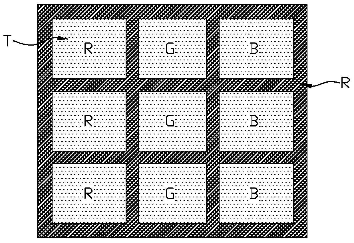
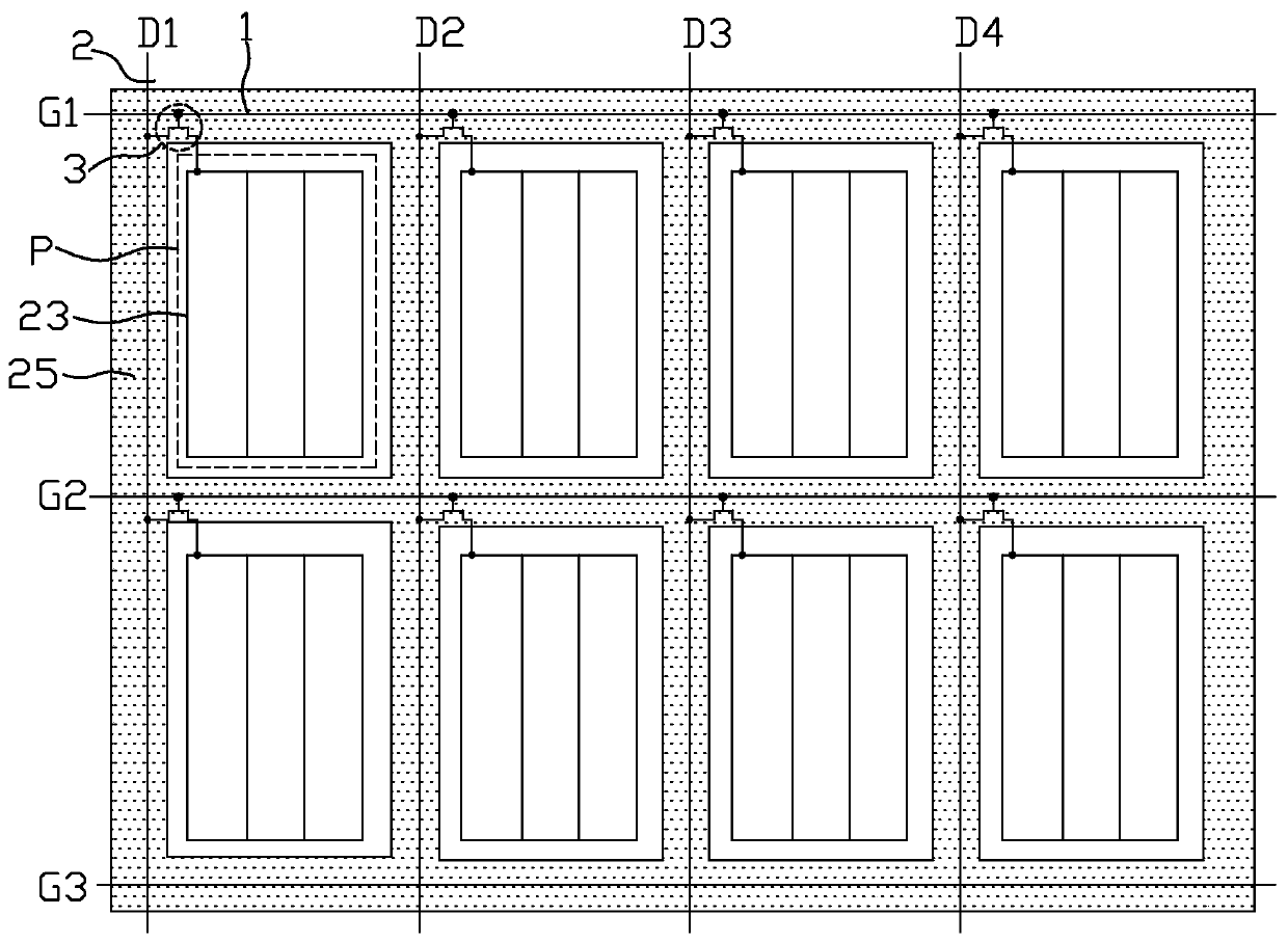
[0038] Such as Figure 1 to Figure 6 As shown, a liquid crystal display panel provided by Embodiment 1 of the present invention includes a first substrate 10 , a second substrate 20 opposite to the first substrate 10 , and a liquid crystal layer between the first substrate 10 and the second substrate 20 30. On the side of the second substrate 20 facing the liquid crystal layer 30, a plurality of scanning lines 1 and a plurality of data lines 2 are mutually insulated and intersected to define a plurality of pixel units P, and each pixel unit P is provided with a pixel electrode 23 and a The thin film transistor 3, the pixel electrode 23 is electrically connected to the scan line 1 and the data line 2 adjacent to the thin film transistor 3 through the thin film transistor 3, wherein the first substrate 10 is a color filter substrate, the second substrate 20 is an array substrate, and the thin film transistor 3 It includes a gate, a source and a drain, and the source and the drai...

Embodiment 2

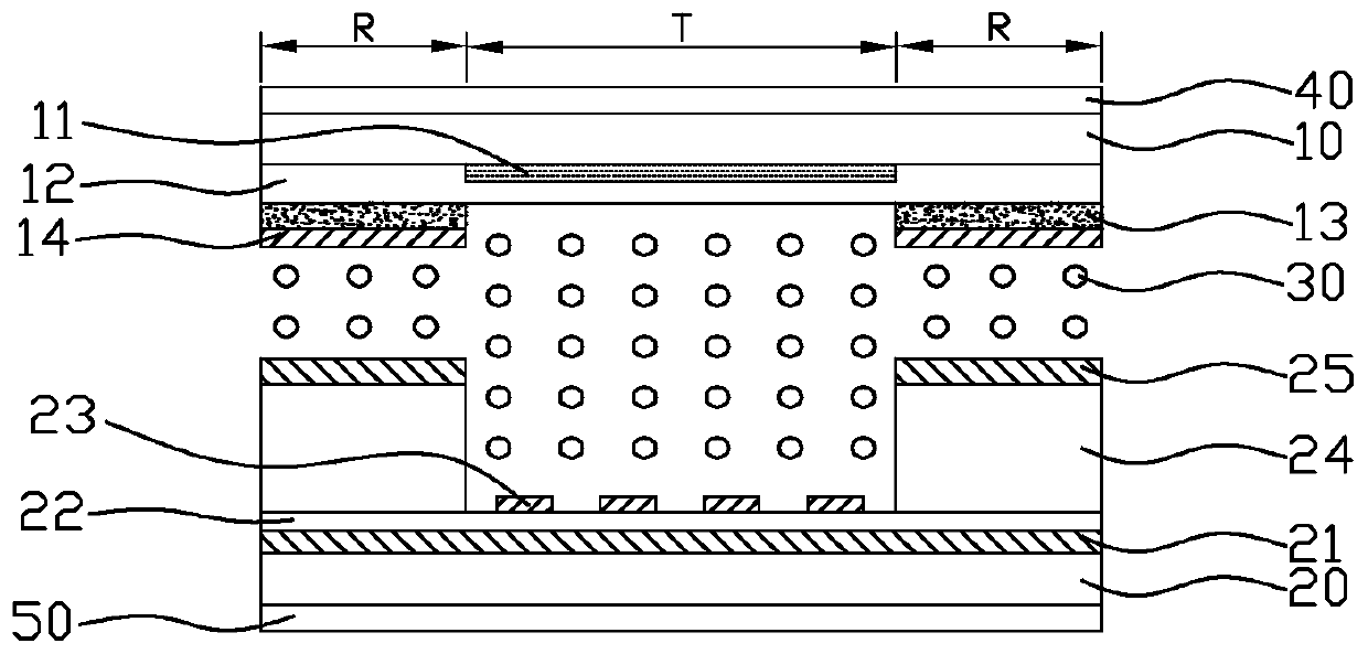
[0053] like Figure 7 As shown, the liquid crystal display panel provided by Embodiment 2 of the present invention is the same as Embodiment 1 ( Figure 5 ) in the liquid crystal display panel is basically the same, the difference is that, in this embodiment, the first quarter-wave plate 13 is a full-surface structure, and the second substrate 20 is also provided with a second quarter-wave plate of the entire surface A wave plate 26 , the fast and slow axes of the second quarter wave plate 26 and the second light transmission axis X2 of the second polarizer 50 form an angle of 45°. Because, using the whole first quarter-wave plate 13, it is necessary to attach a second quarter-wave plate 26 corresponding to the first quarter-wave plate 13 on the side of the second substrate 20, so that the transmission will not be affected. Normal display of zone T. Certainly, the second quarter-wave plate 26 only needs to correspond to the transmission region T, but this will increase the e...

Embodiment 3

[0058] like Figure 8 As shown, the liquid crystal display panel provided by Embodiment 3 of the present invention is the same as Embodiment 2 ( Figure 7 ) in the liquid crystal display panel is basically the same, the difference is that, in this embodiment, the first quarter wave plate 13 is arranged between the first substrate 10 and the first polarizer 40, the second quarter wave plate The wave plate 26 is arranged between the second substrate 20 and the second polarizer 50. Of course, the first quarter-wave plate 13 and the second quarter-wave plate 26 can also be arranged on other layers according to actual needs, for example , the first quarter-wave plate 13 is disposed between the first substrate 10 and the color-resist layer 11, and the second quarter-wave plate 26 is disposed between the second substrate 20 and the common electrode 21. limit.

[0059] Compared with Embodiment 2, in this embodiment, the first quarter-wave plate 13 is arranged outside the liquid crys...


PUM


Abstract

The invention discloses a liquid crystal display panel. The liquid crystal display panel comprises a first substrate, a second substrate and a liquid crystal layer, wherein the second substrate is opposite to the first substrate; the liquid crystal layer is located between the first substrate and the second substrate; a first polaroid is arranged on the first substrate; a second polaroid is arranged on the second substrate; a first quarter-wave plate is arranged on the first substrate; a speed shaft of the first quarter-wave plate forms a 45-degree angle with a first transmitting shaft of thefirst polaroid; a reflecting electrode is arranged on the second substrate; an auxiliary electrode opposite to the reflecting electrode is arranged on the first substrate; the area, corresponding to the reflecting electrode, of the liquid crystal display panel is a reflecting area; the area, corresponding to each pixel unit, of the liquid crystal display panel is a transmitting area; and the thickness of the liquid crystal layer corresponding to the reflecting area is a half of the thickness of the liquid crystal layers corresponding to the transmitting areas. The switching between specular reflection and transmission is realized through controlling the corresponding liquid crystal molecules int the reflecting area to switch between a flat lying posture and a standing posture. The invention further comprises a driving method and a liquid crystal display device.

Description

technical field [0001] The invention relates to the technical field of liquid crystal display, in particular to a liquid crystal display panel, a driving method thereof, and a liquid crystal display device. Background technique [0002] With the development and progress of liquid crystal display technology, people have higher and higher requirements for liquid crystal display devices. At present, a display device that can be used as a mirror and also has a display function is very popular, that is, a mirror display device. [0003] The preparation of existing mirror display devices usually adopts a layer of semi-reflective and semi-permeable film on the outgoing light of the display panel. When displaying, the light from the backlight passes through the display panel to form a color picture for display; when the display is completed Finally, at this time, the light from the external environment is irradiated on the semi-reflective and semi-permeable film to realize the mirro...

Claims


Application Information

Patent Timeline
IPC IPC(8): G02F1/1335G02F1/1343G02F1/133
CPCG02F1/133528G02F1/134309G02F1/13439G02F1/133
Inventor 薛兴皓
Owner KUSN INFOVISION OPTOELECTRONICS
Why Eureka
Try Eureka