Multipath parallel photoelectric module structure and assembly method thereof

The technology of a photoelectric module and assembly method, which is applied in the coupling of optical waveguides, can solve the problems of high cost of optical interconnection and cumbersome optical alignment process, and achieve the goal of reducing cost and process difficulty, and simplifying the structure of optical interconnection Effect

Inactive Publication Date: 2010-12-22
INST OF MICROELECTRONICS CHINESE ACAD OF SCI
View PDF0 Cites 4 Cited by
  • Summary
  • Abstract
  • Description
  • Claims
  • Application Information

AI Technical Summary

Problems solved by technology

Because the size of these mirrors and microlenses is as small as microns, the alignment accuracy requirements are very strict, and their assembly and tedious optical alignment process have become important reasons for the high cost of optical interconnection

Method used


Image

  • Multipath parallel photoelectric module structure and assembly method thereof
  • Multipath parallel photoelectric module structure and assembly method thereof
  • Multipath parallel photoelectric module structure and assembly method thereof

Examples


Embodiment Construction

[0025] In order to make the object, technical solution and advantages of the present invention clearer, the present invention will be described in further detail below in conjunction with specific embodiments and with reference to the accompanying drawings.

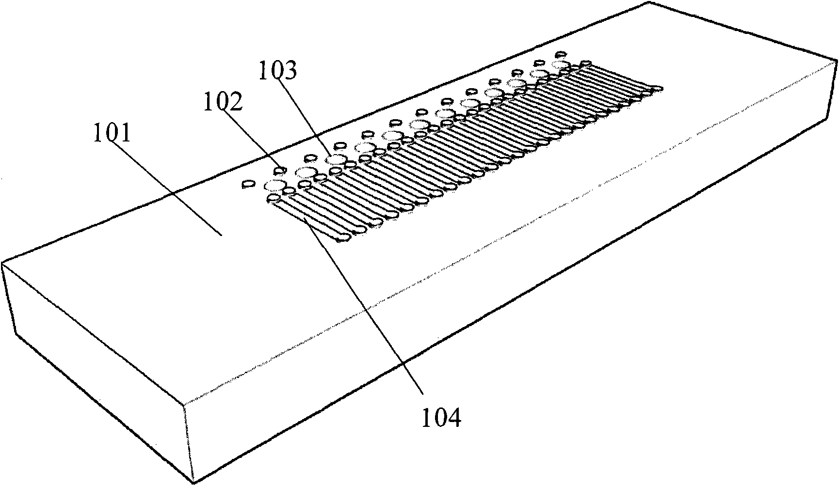
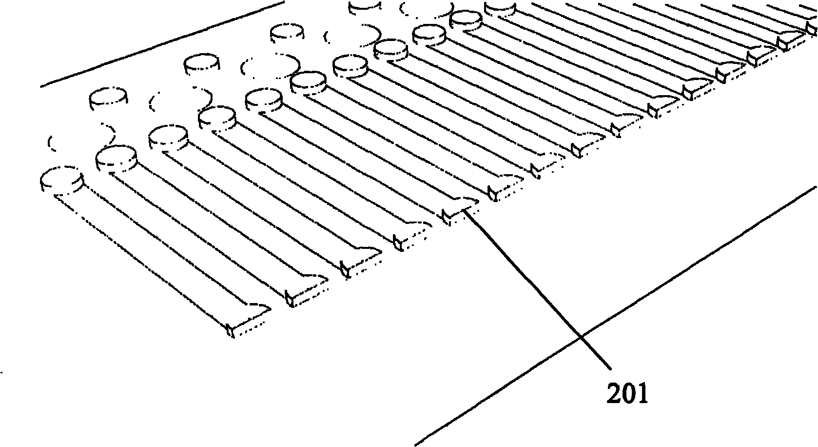
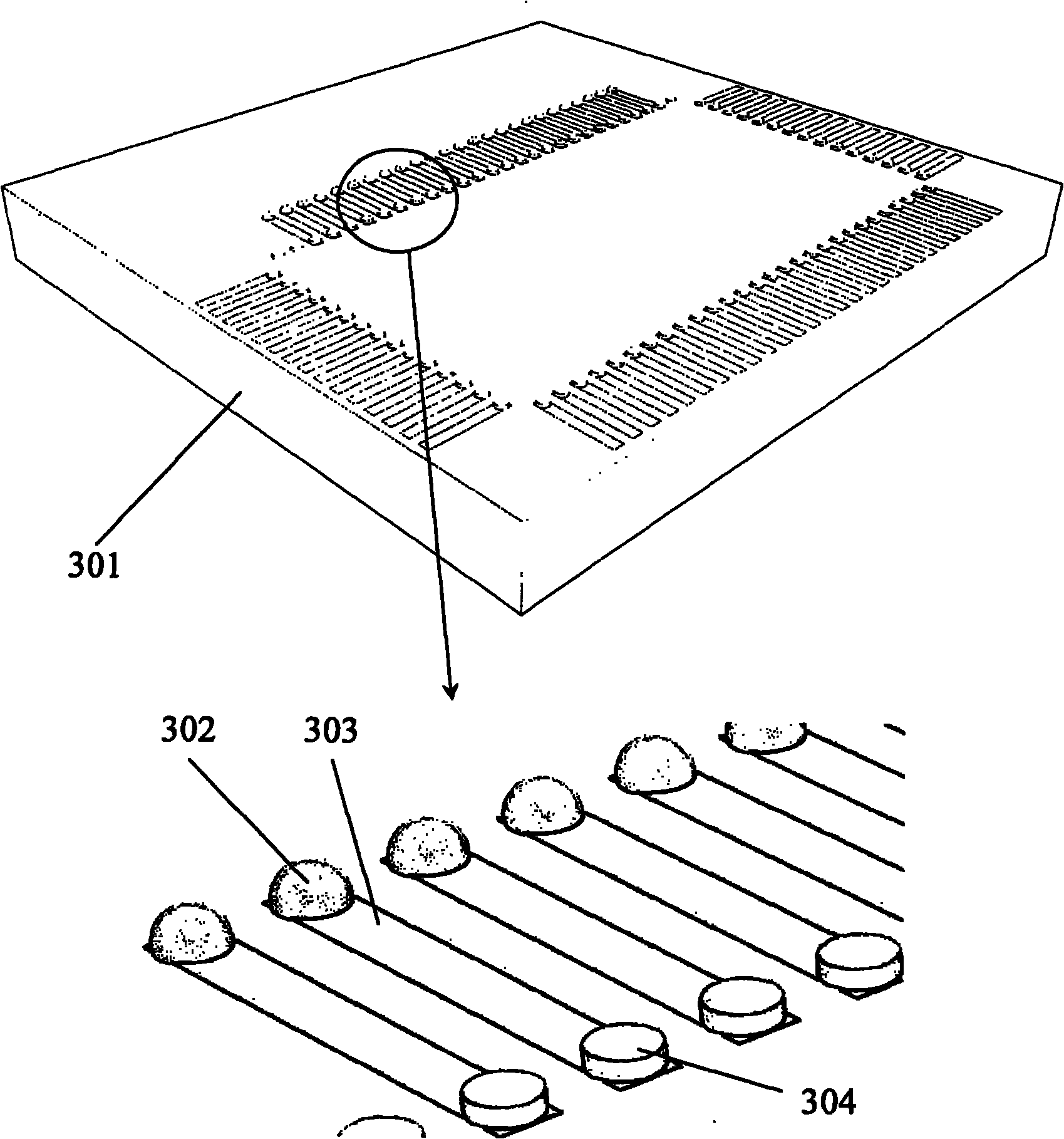
[0026] The multi-channel parallel photoelectric module structure provided by the present invention includes two carriers assembled vertically to each other. Wherein the photoelectric device is installed on the first carrier, and the driving (receiving) chip is installed on the second carrier. There are circuit wiring on the surface of the two carriers, electrodes or pads on the terminals, and solder bumps on the pads, which are used for assembling optoelectronic devices and vertical assembly of the two carriers. The two carriers are assembled perpendicular to each other, and the solder bumps on the edge of the first carrier contact and connect with the solder bumps on the second carrier.

[0027] The assembly method of t...


PUM


Abstract

The invention relates to the very short optical interconnection technology and the electronic packaging fields, and discloses a multipath parallel photoelectric module assembly structure. The assembly method of the structure comprises the following concrete steps: assembling a photoelectrical conversion device in a multipath parallel photoelectric module and a driving (receiving) chip on two ground slides respectively, and assembling and electrically connecting the two ground slides in a mutually perpendicular mode so as to enable the light emitting (light receiving) surface of the photoelectric device to be vertical to a baseplate plane on which the driving (receiving) chip is arranged, thereby lowering the height of the photoelectric module and meeting the requirements of an electronic system on high density and small volume. The structure can be used for preparing an independent photoelectric transceiving module, and can be further coupled with planar optical waveguide, thus realizing mid-plate optical interconnection of light paths without transition.

Description

technical field [0001] The invention relates to the field of very short-distance multi-channel parallel optical interconnection technology and electronic packaging, in particular to a multi-channel parallel photoelectric module structure and an assembly method thereof. Background technique [0002] Interconnect technology is an important part of electronic technology. With the development of various high-performance devices such as supercomputers, high-end servers, and core routers, higher requirements are placed on interconnection bandwidth. Optical interconnection can overcome the physical bottleneck of electrical interconnection in high-speed data transmission, and it is the development trend of high-speed interconnection technology. [0003] Optical interconnection involves photoelectric conversion, which involves many components, such as: lasers, photodetectors, laser driver chips, detector signal amplification chips, optical fibers or optical waveguides, etc. With th...

Claims


Application Information

Patent Timeline
IPC IPC(8): G02B6/42
Inventor 李志华万里兮
Owner INST OF MICROELECTRONICS CHINESE ACAD OF SCI
Why Eureka
Try Eureka