Multi-chip 3D packaging structure and manufacturing method thereof

A technology of packaging structure and manufacturing method, applied in semiconductor/solid-state device parts, semiconductor devices, electrical components, etc., can solve problems affecting product performance, restricting product miniaturization, etc., and achieve the effect of reducing process difficulty and cost

Active Publication Date: 2022-03-01
SIPLP MICROELECTRONICS CHONGQING CO LTD
View PDF0 Cites 0 Cited by
  • Summary
  • Abstract
  • Description
  • Claims
  • Application Information

AI Technical Summary

Problems solved by technology

Packaging technology not only affects the performance of the product, but also restricts the miniaturization of the product

Method used


Image

  • Multi-chip 3D packaging structure and manufacturing method thereof
  • Multi-chip 3D packaging structure and manufacturing method thereof
  • Multi-chip 3D packaging structure and manufacturing method thereof

Examples


Embodiment Construction

[0085] In order to make the above objects, features and advantages of the present invention more comprehensible, specific embodiments of the present invention will be described in detail below in conjunction with the accompanying drawings.

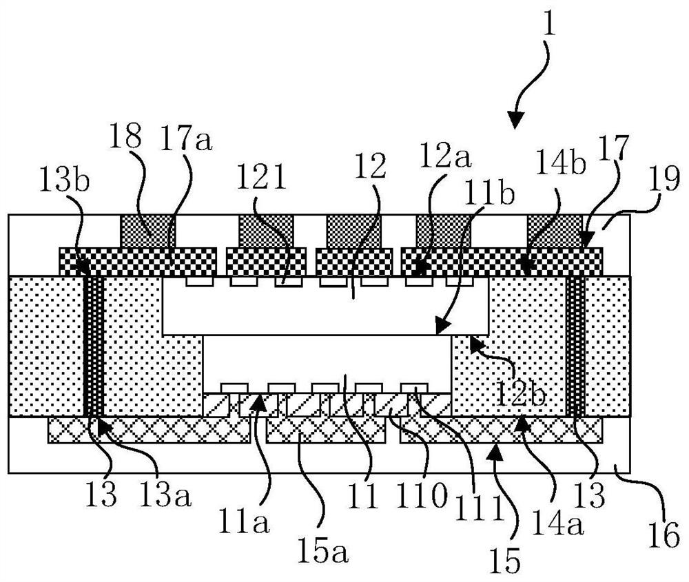
[0086] figure 1 is a schematic cross-sectional structure diagram of the multi-chip 3D packaging structure according to the first embodiment of the present invention.

[0087] refer to figure 1 As shown, the multi-chip 3D packaging structure 1 includes:

[0088] The first die 11 and the second die 12, the first die 11 includes a number of first pads 111, the first pad 111 is located on the active surface 11a of the first die 11, the second die 12 includes a number of second The pad 121, the second pad 121 is located on the active surface 12a of the second die 12; the first die 11 and the second die 12 are arranged back to back;

[0089] The protection layer 110 covers the active surface 11a of the first die 11, and the protection layer 1...


PUM


Abstract

The invention provides a multi-chip 3D packaging structure and a manufacturing method thereof. In the packaging structure, the first bare chip and the second bare chip arranged back to back and the conductive pillars are packaged in the plastic sealing layer, and the first bare chip includes A number of first pads, the active surface of the first die is covered with a protective layer exposing the first pad, and the second bare chip includes a number of second pads located on the active surface; the protective layer, the first pad, the conductive column There is a first rewiring layer on the first end of the first end and the front side of the plastic encapsulation layer to perform circuit layout on each first pad, and the first redistribution layer is led to the back side of the plastic encapsulation layer through conductive pillars; the active surface of the second die , the second end of the conductive column and the back of the plastic encapsulation layer have a second rewiring layer to carry out circuit layout for each second pad, the second rewiring layer is electrically connected to the first rewiring layer through the conductive column, and the second Pins are provided on the redistribution layer. The wiring of the multi-chip 3D packaging structure is more complex, the volume is smaller, and the degree of freedom is higher.

Description

technical field [0001] The invention relates to the technical field of chip packaging, in particular to a multi-chip 3D packaging structure and a manufacturing method thereof. Background technique [0002] In recent years, with the continuous development of circuit integration technology, electronic products are increasingly developing in the direction of miniaturization, intelligence, high integration, high performance and high reliability. Packaging technology not only affects the performance of the product, but also restricts the miniaturization of the product. [0003] In view of this, the present invention provides a multi-chip 3D packaging structure and a manufacturing method thereof, so as to meet the requirements of small volume, compact structure and high integration of the packaging structure. Contents of the invention [0004] The object of the present invention is to provide a multi-chip 3D packaging structure and a manufacturing method thereof, so as to meet ...

Claims


Application Information

Patent Timeline
IPC IPC(8): H01L25/07H01L25/00H01L23/498
CPCH01L25/071H01L25/50H01L23/49838H01L2224/18H01L2224/97
Inventor 霍炎涂旭峰
Owner SIPLP MICROELECTRONICS CHONGQING CO LTD
Why Eureka
Try Eureka