
Buffer structure, display panel and manufacturing method of buffer structure

一种缓冲结构、无机层的技术,应用在半导体/固态器件制造、光伏发电、电气元件等方向,能够解决降低封装膜层抗水氧能力、缩短屏幕使用寿命等问题

Active Publication Date: 2019-11-08
WUHAN CHINA STAR OPTOELECTRONICS SEMICON DISPLAY TECH CO LTD
View PDF5 Cites 2 Cited by
  • Summary
  • Abstract
  • Description
  • Claims
  • Application Information

AI Technical Summary

Problems solved by technology

However, with such stacked packaging layers, the organic layers will be connected together to form a complete water and oxygen channel, which reduces the water and oxygen resistance of the packaging film layer and shortens the service life of the screen.

Method used


Image

  • Buffer structure, display panel and manufacturing method of buffer structure
  • Buffer structure, display panel and manufacturing method of buffer structure
  • Buffer structure, display panel and manufacturing method of buffer structure

Examples


Embodiment Construction

[0037] In describing the present invention, it should be understood that the terms "center", "longitudinal", "transverse", "length", "width", "thickness", "upper", "lower", "front", " Orientation indicated by rear, left, right, vertical, horizontal, top, bottom, inside, outside, clockwise, counterclockwise, etc. The positional relationship is based on the orientation or positional relationship shown in the drawings, which is only for the convenience of describing the present invention and simplifying the description, rather than indicating or implying that the referred device or element must have a specific orientation, be constructed and operated in a specific orientation, Therefore, it should not be construed as limiting the invention. In addition, the terms "first" and "second" are used for descriptive purposes only, and cannot be interpreted as indicating or implying relative importance or implicitly specifying the quantity of indicated technical features. Thus, a feature...


PUM


Abstract

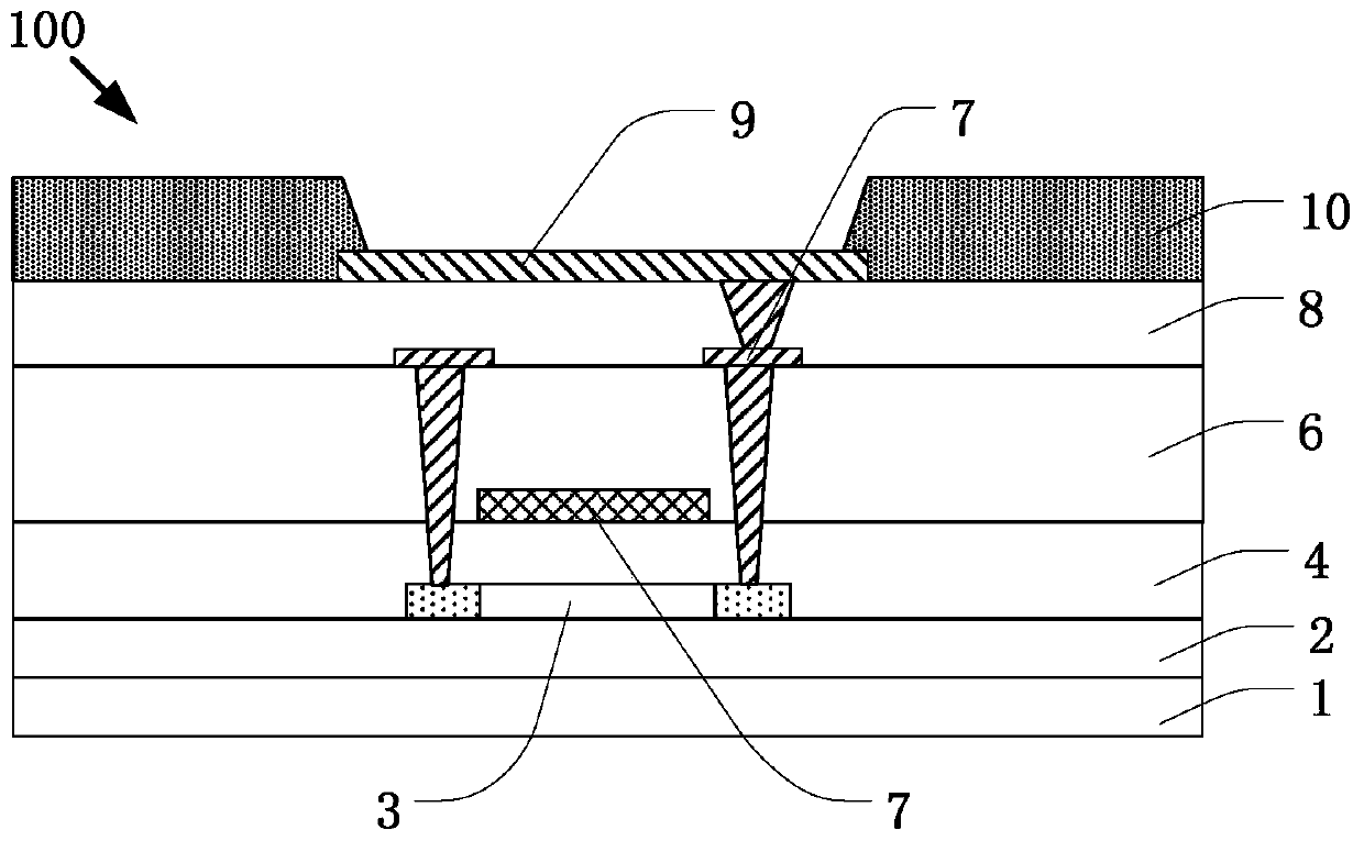
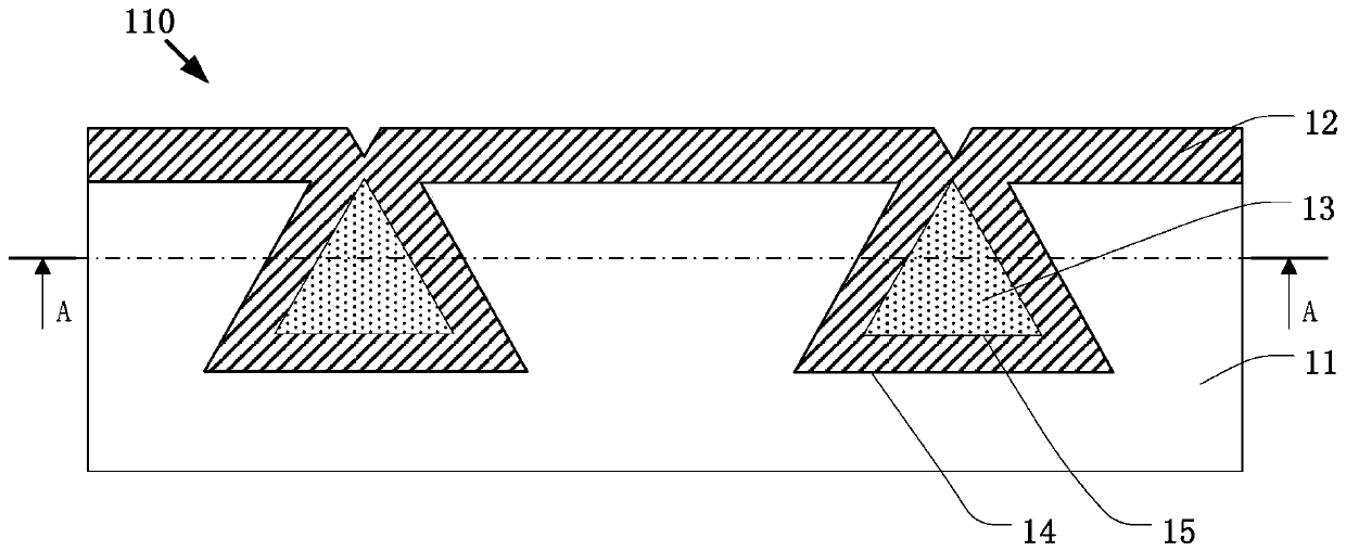
The invention provides a buffer structure, a display panel and a manufacturing method of a buffer structure. The display panel includes at least one buffer structure including a first inorganic layer,a second inorganic layer, and an organic layer. Trapezoidal grooves arranged at intervals are arranged at the surface of one side of the first inorganic layer, the second inorganic layer is arrangedon the surface of one side, provided with the trapezoidal grooves, of the first inorganic layer, covers the surface of the inner side of the trapezoidal grooves and connected at the groove mouths to form a capillary channel; and the organic layer fills the capillary channel. The manufacturing method of a buffer structure comprises the steps of: manufacturing an inorganic layer, a second inorganiclayer and an organic layer. The bending stress of the inorganic layers can be effectively relieved by allowing the organic layer to penetrate the inorganic layers, and the number of times of bending of the display panel is improved without influence of the inorganic layers on the barrier property of water and oxygen.

Description

technical field [0001] The invention relates to the technical field of display panel processing, in particular to a buffer structure, a display panel and a manufacturing method of the buffer structure. Background technique [0002] Organic light-emitting diode (OLED) devices have the advantages of simple structure, fast response, active light emission, and low power consumption, and have been widely used in display fields such as mobile phones, tablets, and televisions. With the development of product differentiation, flexible and folding screens have become a trend. In a flexible OLED device, there are a display part, a driver IC and metal wires connecting the two, wherein the driver IC is distributed on the lower frame of the panel. At present, more and more mobile phone manufacturers are trying to launch bendable mobile phones, requiring the number of screen bends to reach a commercially acceptable level. There are many inorganic films with high stress in the OLED panel...

Claims


Application Information

Patent Timeline
Patent Type & Authority Applications(China)
IPC IPC(8): H01L23/00H01L27/32H01L51/52H01L51/56
CPCH01L23/562H10K59/12H10K50/844H10K59/1201H10K71/00H01L27/1248H01L27/1225Y02E10/549H10K77/111H10K2102/311H10K59/87H01L29/78603H01L29/78654H01L29/78675H01L29/7869
Inventor 王坤
Owner WUHAN CHINA STAR OPTOELECTRONICS SEMICON DISPLAY TECH CO LTD
Learn More