Packaging structure for three-dimensional integration of radio frequency system and design method thereof

A packaging structure, three-dimensional integration technology, applied in computing, special data processing applications, instruments, etc., to achieve the effect of convenient processing and integration, large chip space, and simple processing

Pending Publication Date: 2019-11-19
CHENGDU GANIDE TECH
View PDF0 Cites 13 Cited by
  • Summary
  • Abstract
  • Description
  • Claims
  • Application Information

AI Technical Summary

Problems solved by technology

[0004] In view of the above-mentioned shortcomings in the prior art, the packaging structure and design method for three-dimensional integration of radio frequency systems provided by the present invention solve the problem of wirelessly realizing three-dimensional integration of heterogeneous chips in traditional radio frequency systems

Method used


Image

  • Packaging structure for three-dimensional integration of radio frequency system and design method thereof
  • Packaging structure for three-dimensional integration of radio frequency system and design method thereof
  • Packaging structure for three-dimensional integration of radio frequency system and design method thereof

Examples


Embodiment Construction

[0049] The specific embodiments of the present invention are described below so that those skilled in the art can understand the present invention, but it should be clear that the present invention is not limited to the scope of the specific embodiments. For those of ordinary skill in the art, as long as various changes Within the spirit and scope of the present invention defined and determined by the appended claims, these changes are obvious, and all inventions and creations using the concept of the present invention are included in the protection list.

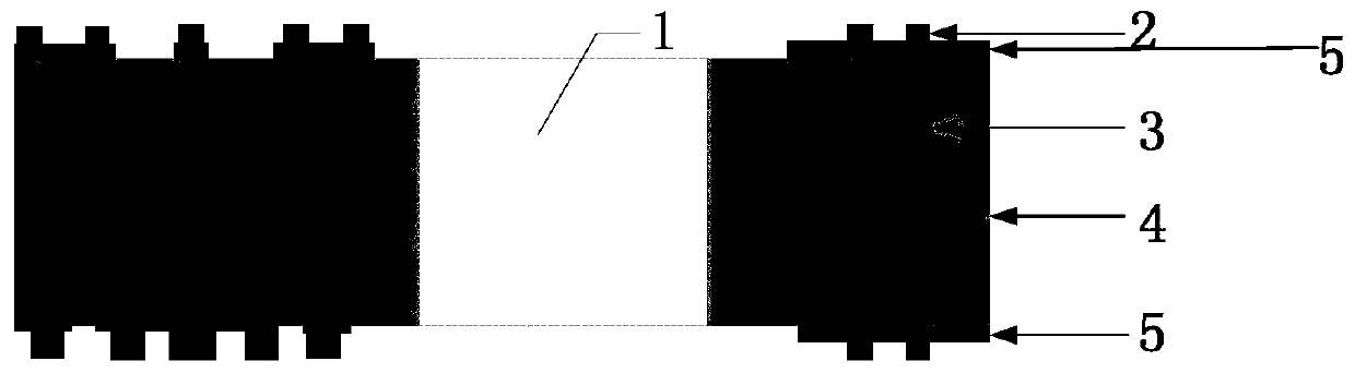
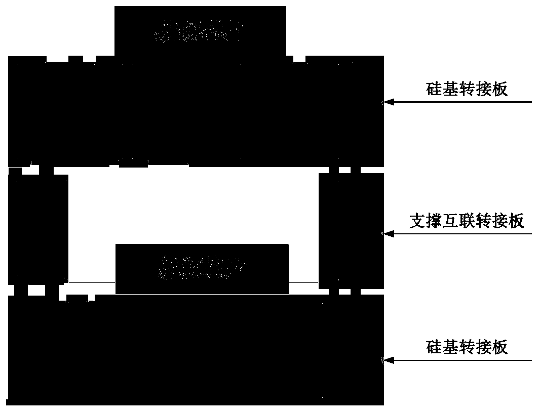
[0050] Such as figure 1 As shown, a packaging structure for three-dimensional integration of radio frequency systems, including silicon-based interposer boards and supporting interconnection interposer boards that are alternately stacked vertically from bottom to top;

[0051] There are at least two supporting interconnection adapter plates, and a cavity 1 is formed between two adjacent supporting interconnection adapter pl...


PUM


Abstract

The invention discloses a packaging structure for three-dimensional integration of a radio frequency system and a design method thereof. The structure comprises a silicon-based adapter plate and at least two supporting interconnection adapter plates which are alternately and longitudinally stacked from bottom to top, wherein a cavity is formed between the at least two supporting interconnection adapter plates; each of the silicon-based adapter plate and the supporting interconnection adapter plates comprises a silicon substrate, a through silicon via (TSV), micro bumps and an RDL wiring layer.The TSV penetrates the silicon substrate; the RDL wiring layers are arranged on the upper surface and the lower surface of the silicon substrate; the micro bumps are arranged on the two RDL wiring layers; the TSV, the RDL wiring layers, and the micro bumps are connected with one another. The structure has the effects of vertical interconnection and structural support, three-dimensional vertical stacking of radio frequency chips can be achieved, and the problem of electromagnetic compatibility during three-dimensional stacking of the radio frequency chips can be solved through flexible design.

Description

technical field [0001] The invention belongs to the technical field of radio frequency system packaging, and in particular relates to a packaging structure for three-dimensional integration of radio frequency systems and a design method thereof. Background technique [0002] In the complex electromagnetic environment of the battlefield, how to better play the role of electronic information equipment and achieve good combat effectiveness has become more difficult, which puts forward higher requirements for the intelligence, miniaturization and light weight of electronic information equipment, and also This puts forward higher requirements for RF system integration. [0003] The common existing RF system integration methods include three-dimensional integration, that is, multiple chips are placed side by side on the substrate, connected by wire bonding, etc., and then packaged in the package; and 2.5D integration that further reduces the volume: multiple Chips are placed side...

Claims


Application Information

Patent Timeline
Patent Type & Authority Applications(China)
IPC IPC(8): H01L21/48H01L23/522G06F17/50
CPCH01L21/4814H01L23/522H01L23/5226
Inventor 胡柳林何舒玮陈依军卢朝保侯杰吴晓东马盛林周鹏胡鑫欣王兵李强斌肖龙
Owner CHENGDU GANIDE TECH
Why Eureka
Try Eureka