Preparation method of PI substrate and display device thereof

A technology for substrates and glass substrates, which is applied in semiconductor/solid-state device manufacturing, photovoltaic power generation, electrical components, etc. It can solve the problems of bubble formation in the film layer, inability to stabilize the bubble control of the PI film layer, and bubble generation in the film layer, etc., to achieve good discharge bubble effect effect

Active Publication Date: 2019-11-22
WUHAN CHINA STAR OPTOELECTRONICS SEMICON DISPLAY TECH CO LTD
View PDF14 Cites 2 Cited by
  • Summary
  • Abstract
  • Description
  • Claims
  • Application Information

AI Technical Summary

Problems solved by technology

[0006] 1. During the processing of the PI substrate, the outside air will invade the material of the PI film layer, thereby forming bubbles inside the film layer;
[0007] 2. The substances in the PI material composed of the PI film layer itself will volatilize, thus

Method used


Image

  • Preparation method of PI substrate and display device thereof
  • Preparation method of PI substrate and display device thereof

Examples


Embodiment Construction

[0043] A method for preparing a PI substrate and a technical solution of a display device thereof according to the present invention will be further described in detail with reference to the accompanying drawings and embodiments.

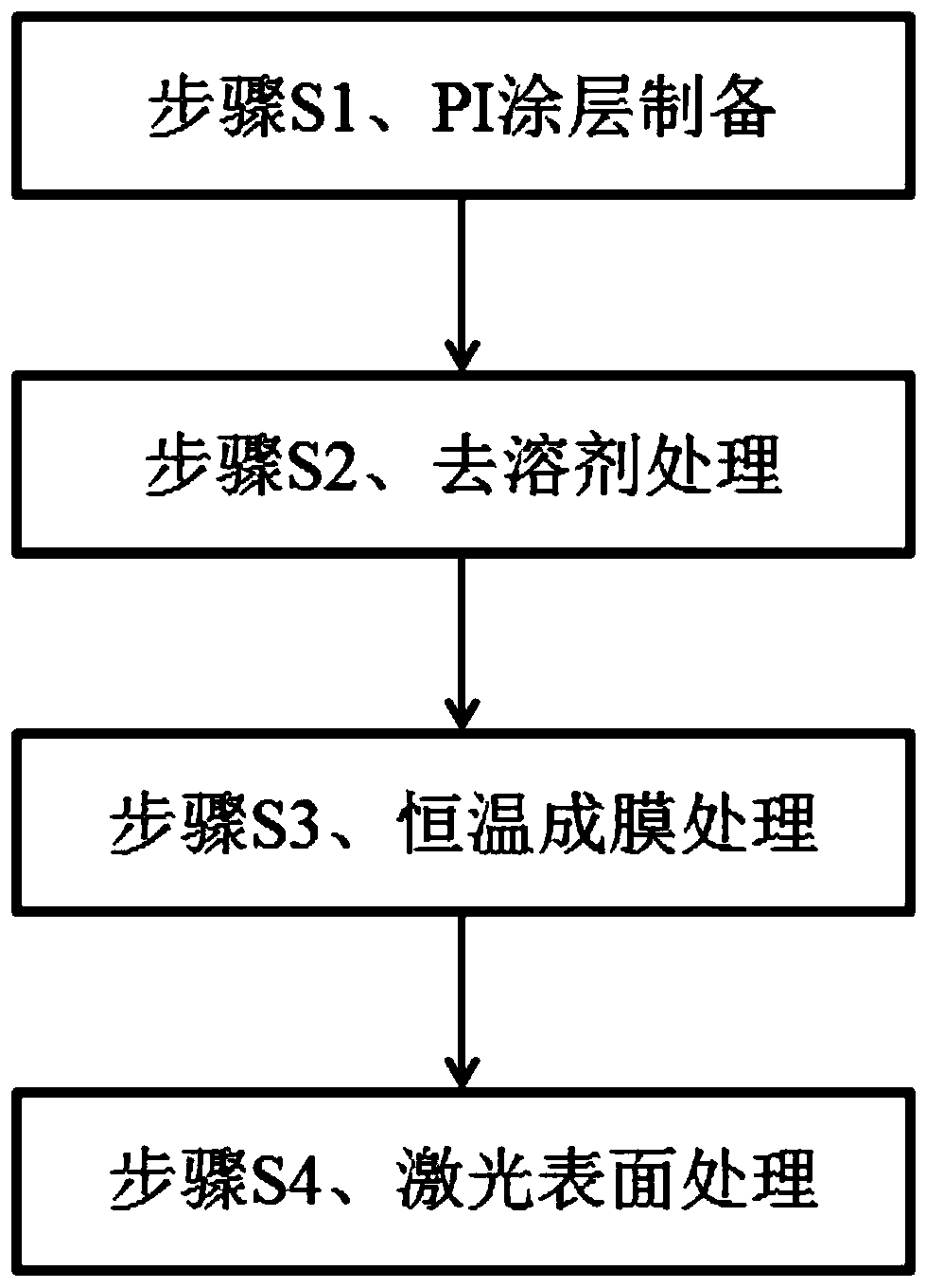
[0044] see figure 1As shown, one embodiment of the present invention provides a method for preparing a PI substrate, which includes a PI coating preparation step S1, a solvent removal treatment step S2, a constant temperature film formation treatment step S3, and a laser treatment surface step S4.

[0045] Each step will be described in detail below.

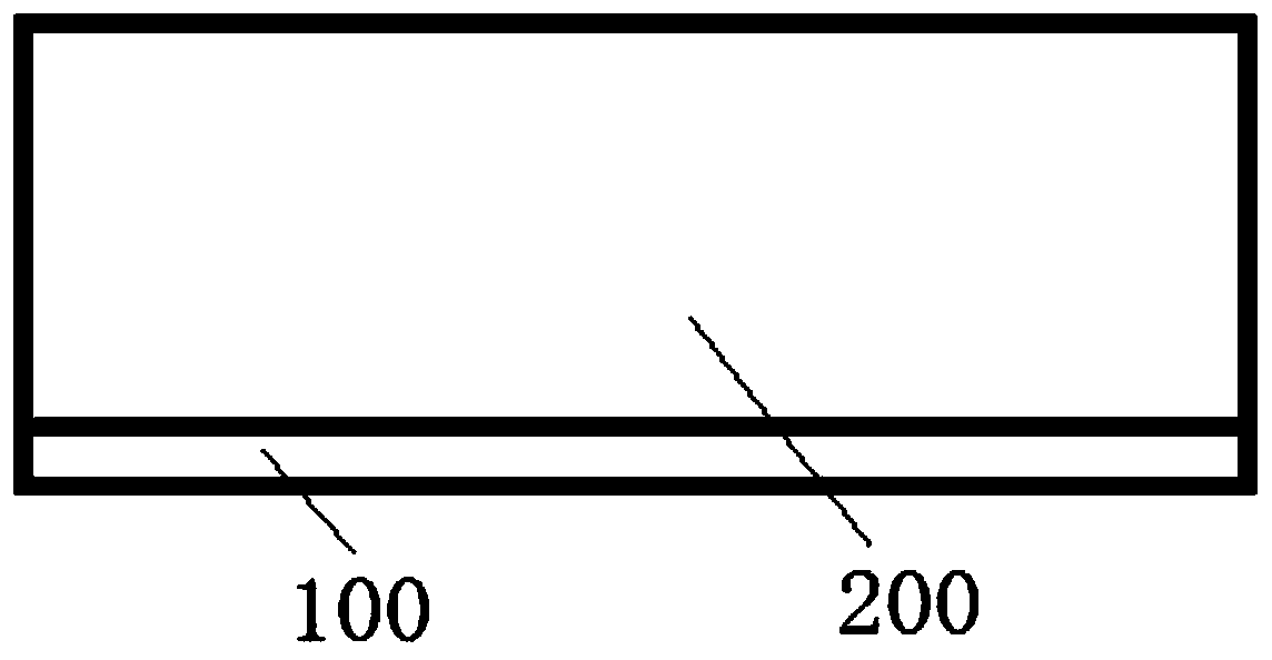
[0046] Step S1, PI coating preparation, which is to provide a glass substrate, and coat a layer of PI material solution on the glass substrate to form a PI coating on the surface of the substrate. The glass substrate used therein is generally, but not limited to, a silicon glass substrate. The PI material solution involved in use is also various PI materials known in the industry that can be used fo...


PUM


Abstract

The invention provides a preparation method of a PI substrate. The preparation method comprises a PI coating preparation step S1, a solvent removal treatment step S2, a constant-temperature film forming treatment step S3 and a laser surface treatment step S4. According to the invention, laser surface treatment is carried out on the PI film layer, when irradiation laser irradiates the surface of the PI film layer, heating treatment can be formed in the PI film layer, bubbles in the PI film layer are heated to go upwards and then are released from the surface of the PI film layer, and thereforePI bubbles existing in the PI film layer in the PI substrate prepared through the preparation method are few.

Description

technical field [0001] The present invention relates to the field of planar display technology, in particular, a method for preparing a PI substrate and a display device thereof. Background technique [0002] It is known that with the continuous development of display technology, organic light-emitting diode display panels (OLEDs) have self-illumination, low driving voltage, high luminous efficiency, short response time, high definition and contrast, nearly 180° viewing angle, and operating temperature range. Wide, and many advantages such as flexible display and large-area full-color display, make it widely used in the fields of display, lighting, and smart wearables. [0003] Moreover, for this kind of OLED display panel, its foldable performance makes its advantages over LCD display panels more obvious. The basis for realizing the foldability of the flexible OLED display panel is that it uses a foldable flexible PI substrate. [0004] Furthermore, for flexible PI substr...

Claims


Application Information

Patent Timeline
IPC IPC(8): H01L51/00H01L27/32
CPCH10K59/00H10K71/00H10K71/80H10K77/111Y02E10/549
Inventor 沈海洋
Owner WUHAN CHINA STAR OPTOELECTRONICS SEMICON DISPLAY TECH CO LTD
Why Eureka
Try Eureka